SHUOQIANG ELECTRONICS
+86 136 0306 3656
info@sqpcb.com
HOME
PCB QUOTE
PRODUCTS
Rigid flex PCB and special PCB
Multilayer PCB
Aluminum base PCB
PCB Mounting and Soldering
Recommend
EQUIPMENTS
CAPABILITY
NEWS
Industry News
Company News
Product Dynamics
FAQ
CONTACT US
HOME
PCB QUOTE
PRODUCTS
Rigid flex PCB and special PCB
Multilayer PCB
Aluminum base PCB
PCB Mounting and Soldering
Recommend
EQUIPMENTS
CAPABILITY
NEWS
Industry News
Company News
Product Dynamics
FAQ
CONTACT US
English
Arabic
Chinese (Simplified)
Dutch
English
French
German
Italian
Portuguese
Russian
Spanish
-->
NEWS & BLOG
Check out the news about us
Home
>
Post Tag
>
PCB Manufacturing
2026-03-09
64
How Much Electricity Does It Take to Produce 1 Square Meter of Double-Sided PCB manufacturing?
Introduction: With 25 years of experience in the PCB manufacturing industry, we often receive questions from peers and downstream customers about the electricity consumption of double-sided PCB production. This article shares real production data, statistical premises, influencing factors, and practical experience from our factory (monthly output 20,000-30,000 square meters), providing a reliable...
Read More
2025-10-31
216
Precision PCB Manufacturing: Preventing Ion Migration with Advanced Technology
Precision PCB Manufacturing: Preventing Ion Migration with Advanced Technology In the world of PCB manufacturing, some design rules are born from hard-earned experience rather than just theoretical calculations. One such critical rule is maintaining a minimum 0.4mm hole-to-hole spacing - a specification that separates temporary prototypes from reliable production-ready boards. Ion Migration: The H...
Read More
2025-10-21
221
Shuoqiang Electronics Paves the Way at the HK Electronics Fair: Driving the Future of FR4 PCB Manufacturing
Shuoqiang Electronics Paves the Way at the HK Electronics Fair: Driving the Future of FR4 PCB Manufacturing In the dynamic and ever-evolving landscape of global electronics, the Hong Kong Electronics Fair stands as a beacon of innovation and opportunity. As one of the world's most anticipated and prestigious trade shows for the electronics industry, it serves as a critical nexus for international...
Read More
2025-09-18
279
The Foundation of Reliability: The Critical Role of PCB Insulation in Electronic Systems
The Foundation of Reliability: The Critical Role of PCB Insulation in Electronic Systems Introduction: Why PCB Insulation Defines Reliability Electronic systems have evolved dramatically over the last five decades, driven by the relentless demand for higher performance, miniaturization, and long-term reliability. In this landscape, PCB insulation plays a foundational role. It is more than just a p...
Read More
2025-09-12
289
What are the Advantages of Reserved Process Edges in Streamlining PCB Production
Introduction and Detailed Explanation of Reserved Process Edges Introduction: The Unseen Enabler in Modern PCB Fabrication In the increasingly competitive landscape of printed circuit board (PCB) manufacturing, engineers constantly look for subtle but effective ways to improve production yield, consistency, and mechanical integrity. One such “quiet hero” is the practice of adding Reserved Process...
Read More
2025-08-09
332
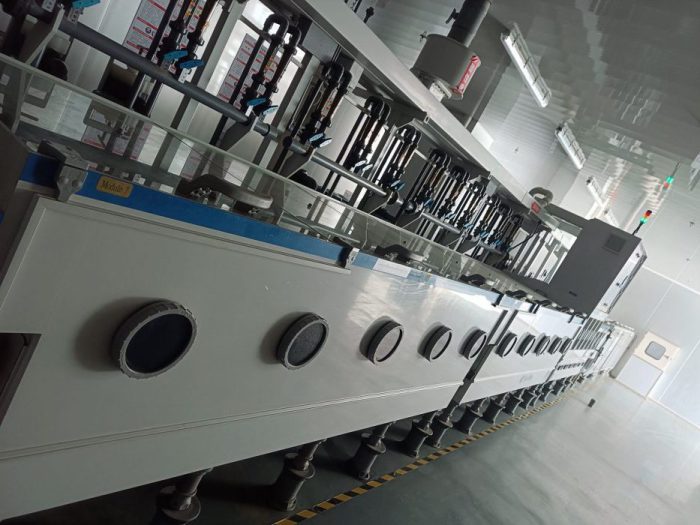
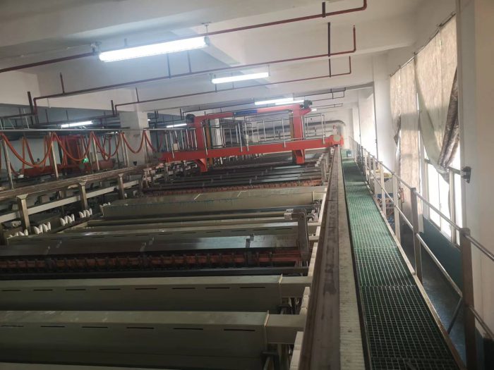
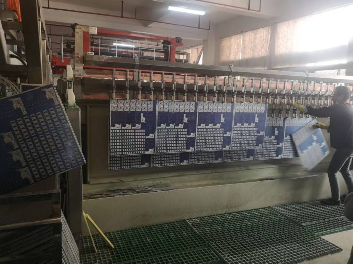
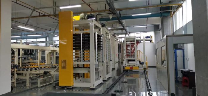
PCB Copper Plating Lines: Manual, Gantry, and Vertical Continuous Systems
PCB Copper Plating Lines Introduction In PCB manufacturing process, copper electroplating is a critical process for building conductive layers and ensuring the durability of the circuit. The efficiency, precision, and stability of this step largely depend on the type of electroplating line used. Today’s factories typically adopt one of three main systems: Manual Copper Plating Lines Gantry (Hoist-...
Read More
2025-08-07
445
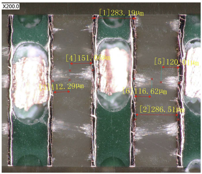
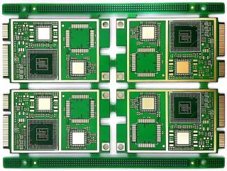
Understanding 2OZ Copper Thickness: IPC Standard vs. Real-World Practice
When customers request a “2OZ copper thickness” for their PCBs, it seems like a straightforward specification. After all, 2OZ copper equates to 70μm in theory. But here's where it gets tricky—once the PCB Manufacturer is manufactured and cross-sectioned, the measured copper thickness often shows just around 60μm, sometimes even lower. This discrepancy frequently causes misunderstandings a...
Read More
2025-02-16
504
PCB Plating Process
PCB Plating Process: Understanding Electroplating in Circuit Board Manufacturing Introduction The PCB plating process, specifically electroplating, is an essential step in printed circuit board (PCB) manufacturing. It enhances the board's conductivity, reliability, and durability by depositing a thin layer of metal, typically copper, onto the PCB surface and through drilled holes. This ensures str...
Read More
2025-02-14
433
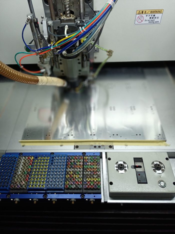
PCB Drilling Speed: The High-Speed Precision of PCB Drilling Machines, Spindle Speed & Drilling Rate
PCB Drilling Speed: The High-Speed Precision of PCB Drilling Machines, Spindle Speed & Drilling Rate Introduction In PCB (Printed Circuit Board) manufacturing, drilling is one of the most high-speed and precision-intensive processes. Modern mechanical and laser drilling machines operate at staggering speeds, ensuring efficient and precise hole creation for vias, through-holes, and microvias. W...
Read More
2025-02-14
465
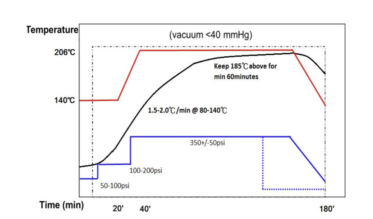
Key Parameters in the PCB Lamination Process In PCB Manufacturing
Key Parameters in the PCB Lamination Process In PCB Manufacturing Introduction The lamination process is a critical step in PCB (Printed Circuit Board) manufacturing, where multiple layers are bonded together under heat and pressure to form a multilayer PCB. Proper control of key lamination parameters ensures reliable adhesion, dimensional stability, and defect-free boards. The three most importan...
Read More
2025-02-13
485
PCB Lamination Process: Key Techniques and Best Practices In PCB Manufacturing
PCB Lamination Process: Key Techniques and Best Practices In PCB Manufacturing Introduction Lamination is a critical process in PCB (Printed Circuit Board) manufacturing, where multiple layers of copper and dielectric materials are bonded together under high temperature and pressure to form a multilayer PCB. The lamination process ensures electrical insulation, mechanical strength, and structural...
Read More
2025-02-13
478
Kraft Paper Role in the Lamination Process in PCB Manufacturing
Kraft Paper Role in the Lamination Process in PCB Manufacturing Introduction Kraft paper plays a crucial role in PCB lamination, serving as a thermal and pressure buffer to ensure uniform heating, controlled cooling, and even pressure distribution. It helps to minimize defects, such as warping, delamination, and pressure-induced indentations, which can significantly affect PCB quality. Despite rec...
Read More
1
2
3
›
NEWS LIST
Industry News
Company News
Product Dynamics
Faq
manufacturer
Product Center
long board pcb
Flexible PCBs
Special PCB
Express Printed Circuit Board
Pcb Prototype
LED PCB
PCB
Printed Circuit Board
Pcb meaning
Pcb manufacturer
Rigid pcb board
Rigid Flex PCB
Contact Us
+86 136 0306 3656
info@sqpcb.com
Get A Quote
g01IcT
Quote
Name:
E-mail:
Your Message:
Submit
E-mail
info@sqpcb.com
Whatsapp
+86 136 0306 3656

 Quote
Quote
 E-mail