


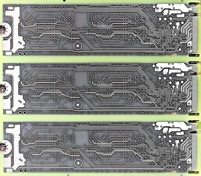


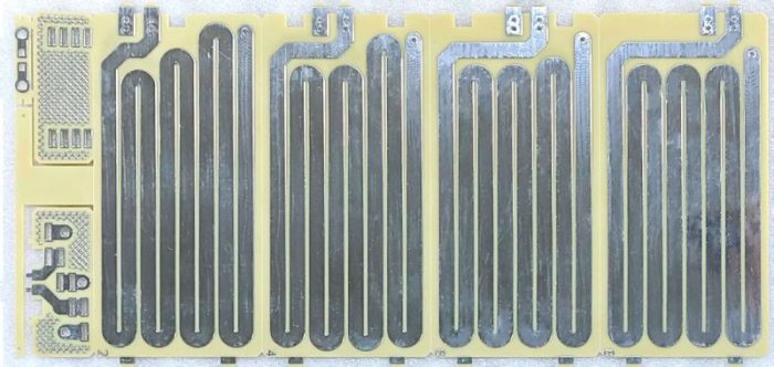


PCB Prototype Manufacturing for Design Verification
A PCB prototype is a small quantity of printed circuit boards manufactured before mass production. It allows engineers to verify circuit performance, PCB dimensions, component placement, assembly compatibility, thermal behavior, and overall product reliability.
A prototype PCB should represent the intended production board as closely as possible. Using the same material, layer stack-up, copper thickness, surface finish, impedance requirements, and critical tolerances provides more meaningful test results and reduces unexpected problems during mass production.
SQPCB supports PCB prototype manufacturing for product development, design verification, engineering testing, customer samples, certification, and pre-production evaluation.
Why Is PCB Prototyping Important?
Producing PCB prototypes before volume manufacturing can help customers:
- Verify the electrical function of a new design
- Check PCB dimensions and mechanical fit
- Confirm component footprints and hole sizes
- Evaluate signal integrity and controlled impedance
- Test thermal performance and current-carrying capability
- Identify DFM and assembly risks
- Complete customer approval or product certification
- Reduce expensive modifications during mass production
Even when a circuit design works correctly in software, actual manufacturing and assembly may reveal issues involving pad dimensions, hole tolerances, solderability, heat dissipation, component clearance, or mechanical installation.
A small prototype order provides an opportunity to correct these problems before larger quantities are produced.
PCB Prototype Types We Support
Our PCB prototype service supports a wide range of board constructions, including:
- Single-sided PCB prototypes
- Double-sided PCB prototypes
- Multilayer PCB prototypes
- Standard FR-4 PCBs
- High-Tg PCBs
- Aluminum-based PCBs
- Copper-based PCBs
- Heavy-copper PCBs
- High-frequency PCBs
- Controlled-impedance PCBs
- HDI and via-in-pad PCBs
- Rigid-flex and special PCB prototypes
Special materials, blind or buried vias, resin-filled vias, heavy copper, unusual board thicknesses, and other advanced processes are evaluated according to the design files and required delivery time.
Available surface finishes include lead-free HASL, HASL with lead, ENIG, OSP, hard gold, and other finishes depending on the application.
Fast PCB Prototype Lead Time
For qualified and fully confirmed orders, typical prototype production capability includes:
- Single-sided and double-sided PCB prototypes: as fast as 24 hours
- 4-layer and 6-layer PCB prototypes: as fast as 3 days
- Complex multilayer and special PCB prototypes: evaluated according to materials and processes
The production schedule begins after the Gerber files, manufacturing specifications, engineering questions, and order details have been confirmed.
Material availability, copper thickness, surface finish, special tolerances, impedance requirements, quantity, and additional processes may affect the final lead time.
PCB Prototype Manufacturing Process
1. File and Engineering Review
Our engineering team checks the Gerber files, drill files, board outline, material, layer count, copper thickness, surface finish, and special requirements.
Potential manufacturing risks are communicated before production begins.
2. CAM and DFM Preparation
The design is reviewed for minimum line width and spacing, annular rings, hole sizes, copper-to-edge distance, solder mask openings, impedance structures, panelization, and other manufacturing details.
3. PCB Fabrication
The prototype follows the required manufacturing processes, including imaging, etching, drilling, copper plating, lamination, solder mask, legend printing, surface finishing, routing, and electrical testing.
4. Quality Inspection
Inspection requirements are selected according to the PCB construction and may include:
- Inner- and outer-layer AOI
- Hole-plating and copper-thickness inspection
- Solder mask registration inspection
- Surface-finish inspection
- Electrical continuity and isolation testing
- Board dimensions and outline inspection
- Final visual inspection
5. Packaging and Delivery
After final inspection, the boards are vacuum-packed or appropriately protected and prepared for international shipment.
For an urgent project, customers should provide the delivery destination and required arrival date so that production and transportation time can be evaluated together.
Prototype PCB Quality Should Match the Application
A prototype is not necessarily a temporary or lower-quality PCB.
When the purpose is to verify the final product, the prototype should use production-representative specifications wherever possible. Changing FR-4 grade, copper thickness, stack-up, surface finish, or impedance structure may reduce the value of the test results.
For example:
- High-current products should use the intended copper thickness.
- High-frequency products should use the specified laminate.
- BGA and fine-pitch designs should use the intended surface finish.
- Controlled-impedance boards should use an approved stack-up.
- High-temperature products should use the required Tg and thermal-performance material.
Our engineering team can review the manufacturing data and help identify specifications that may influence prototype performance or future mass production.
From PCB Prototype to Mass Production
After the prototype has been assembled and tested successfully, the same manufacturing data can be used as the basis for pilot production and volume orders.
Working with one PCB supplier from prototype through mass production can help maintain consistency in:
- Material selection
- Layer stack-up
- Copper thickness
- Surface finish
- Impedance requirements
- Hole and outline tolerances
- Inspection standards
- Engineering records
This reduces repeated communication and helps make the transition from product development to mass production more efficient.
Information Required for a PCB Prototype Quote
To receive an accurate quotation, please provide:
- Gerber or ODB++ files
- NC drill files
- Layer count
- PCB dimensions
- Material requirements
- Finished board thickness
- Inner- and outer-layer copper thickness
- Surface finish
- Solder mask and legend colors
- Quantity
- Impedance or stack-up requirements
- Special processes and tolerances
- Delivery destination
- Required arrival date
If some specifications have not yet been confirmed, send us the available files for engineering review.
Request a PCB Prototype Quote
Send your PCB files and requirements to info@sqpcb.com.
SQPCB provides fast engineering response, flexible prototype quantities, direct technical communication, and manufacturing support from the first prototype through volume production.
A well-manufactured PCB prototype does more than verify a circuit—it helps reduce development risk and prepares the product for reliable mass production.
 Quote
 E-mail