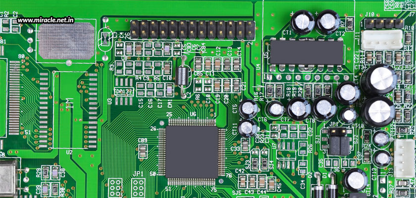
Printed Circuit Boards (PCBs), also known as PCB boards, are the foundation of modern electronic products. From smartphones and industrial control systems to automotive electronics and medical equipment, almost every electronic device depends on a reliable PCB board to connect and control electrical components.
Creating a high-quality PCB board is not only a manufacturing process but also a combination of engineering knowledge, material selection, precision manufacturing, and strict quality control. A professional PCB manufacturer must balance design requirements, electrical performance, reliability, and production efficiency to deliver stable circuit boards for different applications.

The design of a printed circuit board (PCB board) starts with understanding the requirements of the final electronic product.
PCB designers need to consider many factors, including:
Circuit complexity
Signal integrity requirements
Power distribution
Thermal management
Mechanical dimensions
Operating environment
The designer first creates a schematic that defines the electrical connection between components. After completing the schematic design, the next step is PCB layout, where engineers determine the position of components, routing paths, copper layers, and board structure.
The PCB material selection is also a critical decision. Different applications require different PCB materials, such as:
FR-4 PCB for general electronic applications
High Tg PCB for high-temperature environments
Aluminum PCB for LED and thermal management applications
Rogers high-frequency PCB for RF and communication products
Ceramic PCB for advanced thermal performance requirements
A suitable PCB board material directly affects reliability, signal performance, heat dissipation, and product lifetime.
Once the PCB design is completed, the manufacturing process begins.
PCB manufacturing requires precise control of multiple processes, including inner layer fabrication, lamination, drilling, copper plating, circuit imaging, solder mask application, surface finishing, and electrical testing.

Stage 1 of PCB Board manufacturing process including PCB design, material selection, and inner layer fabrication.
The PCB manufacturing process starts with selecting suitable raw materials based on application requirements.
Common PCB materials include:
FR-4 for standard electronic applications
High Tg materials for high-temperature environments
Rogers materials for high-frequency circuits
Aluminum substrates for thermal management applications
For multilayer PCB boards, inner layer fabrication is the first critical manufacturing step.
The copper pattern is transferred onto the inner layer material through imaging and etching processes.
After circuit formation, Automated Optical Inspection (AOI) is used to detect possible defects such as open circuits, shorts, and pattern abnormalities before lamination.
For multilayer PCB boards, multiple copper layers, prepreg, and core materials are stacked according to the designed layer structure.
The lamination process uses controlled temperature and pressure to bond all layers into a single PCB structure.
A stable lamination process is essential because it directly influences:
Layer alignment
Impedance performance
Copper-to-material bonding strength
Thermal reliability
Resistance to delamination
For high-reliability applications, PCB manufacturers must carefully control press parameters, material selection, and stack-up design.

Stage 2 covers PCB Board lamination, drilling, PTH plating, and outer layer circuit formation.
After lamination, PCB drilling creates holes required for electrical connections and component assembly.
PCB drilling requires precise control of:
Hole size tolerance
Drilling accuracy
Aspect ratio
Tool wear management
Different PCB designs may require:
Through holes
Blind vias
Buried vias
Microvias for HDI PCB
The drilling quality directly affects plating reliability and long-term electrical performance.
After drilling, the holes must be plated with copper to create electrical connections between different PCB layers.
The main processes include:
Desmear treatment
Chemical copper deposition
Electrolytic copper plating
The copper thickness inside the hole wall is a critical reliability factor, especially for multilayer PCB boards used in thermal cycling environments.
The circuit pattern is transferred onto the copper surface through imaging technology.
Traditional PCB manufacturing uses film exposure, while modern PCB factories increasingly adopt:
Laser Direct Imaging (LDI) technology
because it provides:
Higher registration accuracy
Better fine-line capability
Reduced film expansion errors
Improved production consistency
After imaging, unwanted copper is removed through etching to create the final conductive traces.
After circuit formation, solder mask is applied to protect copper traces and prevent solder bridging during assembly.
Common solder mask colors include:
Green
Blue
Black
White
Advanced PCB manufacturers increasingly use solder mask LDI technology to improve alignment accuracy, especially for fine-pitch and high-density PCB designs.

Stage 3 includes solder mask, surface finish, electrical testing, final inspection and PCB Board shipping.
The exposed copper pads require surface finishing to protect against oxidation and improve solderability.
Common PCB surface finishes include:
ENIG (Electroless Nickel Immersion Gold)
HASL (Hot Air Solder Leveling)
OSP
Hard Gold Plating
Immersion Silver
The correct surface finish depends on component requirements, assembly process, reliability expectations, and cost considerations.
Before shipment, every PCB board undergoes inspection and testing to ensure reliability.
Typical PCB testing methods include:
Flying Probe Testing
Electrical Testing
AOI Inspection
Impedance Testing
Microsection Analysis
Reliability Testing
A professional PCB manufacturer does not only manufacture circuit boards but also controls every critical process step to reduce manufacturing risks.
The final stage includes:
Visual inspection
Dimensional inspection
Packaging protection
Customer specification verification
Proper packaging is especially important for preventing moisture absorption, oxidation, and handling damage during transportation.
| PCB Type | Layers | Applications |
|---|---|---|
| Single Layer PCB | 1 | LED, simple electronics |
| Double Layer PCB | 2 | Industrial control |
| Multilayer PCB | 4-20 layers | Automotive, servers |
| HDI PCB | Microvia structure | Mobile, high-density devices |
| Aluminum PCB | Metal substrate | LED, power electronics |
The quality of a PCB board directly affects the reliability and lifetime of the final electronic product.
A poorly manufactured PCB may cause problems such as:
Signal transmission failure
Component overheating
Poor soldering performance
Copper migration
Delamination during thermal cycling
Short circuits or open circuits
Therefore, professional PCB manufacturers apply strict quality control systems throughout the production process.
Typical PCB inspection methods include:
Automated Optical Inspection (AOI)
Electrical Testing
Flying Probe Testing
Impedance Testing
Microsection Analysis
Reliability Testing
Selecting a PCB supplier is not only about price. A reliable PCB manufacturer should provide:
Stable manufacturing capability
Advanced production equipment
Engineering support
Consistent quality control
Fast prototype capability
Experience with complex PCB projects
An experienced PCB manufacturer can help customers optimize PCB designs, reduce manufacturing risks, and improve product reliability.
At Shuoqiang Electronics, we focus on providing reliable PCB manufacturing solutions, including multilayer PCB, HDI PCB, high-frequency PCB, aluminum PCB, heavy copper PCB, and other customized circuit board solutions.
The creation of a printed circuit board is a combination of engineering, technology, and manufacturing expertise. From PCB design and material selection to precision production and quality inspection, every step influences the final performance of the PCB board.
As electronic products continue to become smaller, faster, and more powerful, high-quality PCB manufacturing will remain a critical foundation for modern technology.
By working with an experienced PCB manufacturer, companies can achieve better reliability, improved production efficiency, and long-term product success.
With over 25 years of PCB manufacturing experience, Shuoqiang Electronics supports prototype, small batch, and volume PCB production with reliable quality control.
Contact Shuoqiang Electronics for:
✓ Multilayer PCB
✓ HDI PCB
✓ High Frequency PCB
✓ Aluminum PCB
✓ Heavy Copper PCB
Request a PCB Quote Today
A PCB board is a key component used to mechanically support electronic components and provide electrical connections through copper circuits.
PCB boards are widely used in consumer electronics, automotive systems, industrial controls, medical equipment, communication devices, and power electronics.
A high-quality PCB board improves electrical performance, reliability, and the service life of electronic products.
PCB board manufacturing involves multiple precision processes, including material preparation, inner layer fabrication, lamination, drilling, copper plating, circuit imaging, solder mask application, surface finishing, and electrical testing.
Each process affects PCB reliability, signal performance, and manufacturing quality. Professional PCB manufacturers use advanced equipment and strict process control to ensure consistent production.
The most common PCB material is FR-4 because of its good electrical insulation, mechanical strength, and cost effectiveness.
Depending on application requirements, PCB manufacturers may use:
Material selection directly affects PCB reliability and performance.
Single-layer PCBs have one copper layer and are used for simple electronic products.
Double-layer PCBs have copper layers on both sides, allowing more complex circuit designs.
Multilayer PCBs contain multiple copper layers and are used for advanced applications requiring higher wiring density, better electrical performance, and improved reliability.
A reliable PCB manufacturer should provide stable production capability, advanced equipment, strict quality control, engineering support, and experience with complex PCB projects.
Important factors include manufacturing capability, certifications, inspection systems, communication efficiency, and the ability to support prototype and mass production requirements.
Professional PCB manufacturers perform various inspections before shipment, including:
AOI inspection
Electrical testing
Flying probe testing
Impedance testing
Microsection analysis
These tests help identify defects such as open circuits, shorts, incorrect copper thickness, and layer alignment issues.