Printed Circuit Boards, commonly known as PCBs, are an essential component of modern electronics. They serve as the backbone of almost every electronic device we use, from smartphones and laptops to home appliances and medical equipment. The process of creating a PCB involves a complex interplay of art and science, requiring a deep understanding of materials, design, and manufacturing techniques.
Understanding the Basics of PCB Design
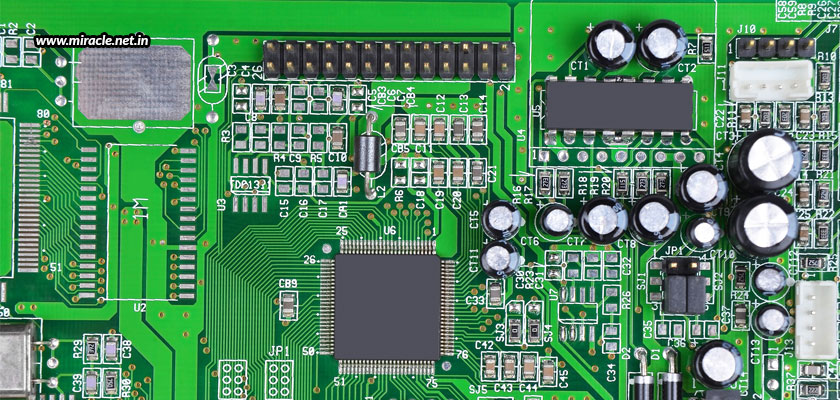
The design of a Printed Circuit Board starts with an understanding of the electronic device it will be used in. The designer must consider factors such as the size and shape of the device, the number of components that will be connected to the board, and the types of signals that will be transmitted. This information is used to create a schematic, a diagram that shows the arrangement of components and the connections between them. Once the schematic is complete, the designer must then choose the appropriate materials for the PCB. This includes the type of substrate, or base material, that will be used, as well as the type of metal that will be used for the conductive pathways, or traces, on the board. The choice of materials will depend on the specific requirements of the device, such as the need for high-temperature resistance, electrical conductivity, or resistance to corrosion.
The Manufacturing Process of PCBs
Once the design of the PCB has been completed, it is time to move on to the manufacturing process. This is where the science of PCB creation takes over, as the designer must ensure that the manufacturing process is precise and consistent, to ensure that the final product is of the highest quality.
The first step in the manufacturing process is to create a photoresist, or negative image, of the PCB design. This is done by projecting the design onto a photosensitive material, which is then developed to create a negative image. The negative image is then used to etch the conductive pathways onto the substrate.
The next step is to apply a thin layer of metal to the substrate, using a process known as metal deposition. This layer of metal will become the conductive pathways on the PCB. The metal deposition process must be carefully controlled to ensure that the metal is of the correct thickness and that there are no defects in the metal layer. Once the metal layer has been applied, the PCB is then subjected to a series of tests, to ensure that it is functioning correctly. This may include tests such as electrical continuity tests, resistance tests, and thermal resistance tests. If any defects are found, they must be corrected before the PCB can be considered ready for use.
The Importance of PCB Quality
It is essential that the quality of the Printed Circuit Board is of the highest standard, as any defects or inconsistencies in the manufacturing process can lead to a range of problems. For example, a poorly manufactured PCB may not be able to handle the high temperatures generated by the electronic components, leading to thermal damage. Similarly, a poorly manufactured PCB may not be able to transmit signals effectively, leading to poor performance or even complete failure of the device. In conclusion, the process of creating a Printed Circuit Board involves a delicate balance of art and science. From the initial design, through to the manufacturing process, it is essential that the highest standards of quality are maintained, to ensure that the final product is of the highest quality. By investing in the art and science of PCB creation, we can ensure that the electronic devices we use every day will continue to perform at their best, for years to come.

- long board pcb
- Flexible PCBs
- Special PCB
- Express Printed Circuit Board
- Pcb Prototype
- LED PCB
- PCB
- Printed Circuit Board
- Pcb meaning
- Pcb manufacturer
- Rigid pcb board
- Rigid Flex PCB
 Quote
Quote
 E-mail