Rogers RO3006 PCB: Properties, Applications and Fabrication Guide
Rogers RO3006 is a ceramic-filled PTFE high-frequency laminate with a relatively high dielectric constant. It is commonly selected for RF and microwave circuits that require compact dimensions, low transmission loss, and reliable plated-through-hole performance.
Its process dielectric constant is 6.15 ± 0.15, which is considerably higher than that of commonly used materials such as RO3003 and RO4350B. For a given frequency and circuit structure, a higher dielectric constant can reduce the wavelength within the material and help decrease the dimensions of certain RF circuit elements.
However, a higher Dk does not mean that Rogers 3006 is better for every high-frequency PCB.
Material selection should also consider:
- Operating frequency
- Impedance and phase requirements
- Insertion loss
- Circuit dimensions
- Laminate thickness
- Copper type and surface roughness
- Operating temperature range
- PCB layer count
- Hybrid or multilayer construction
- Fabrication requirements
- Material availability and lot consistency
RO3006 is a specialized high-frequency material with clearly defined characteristics. Its advantages can only be fully realized when its electrical properties and manufacturing requirements match the actual application.
1. What Is Rogers RO3006?
Rogers RO3006 belongs to the RO3000® family of high-frequency circuit materials. It is a ceramic-filled, non-woven-glass-reinforced PTFE composite.
The RO3000 series adopts varied ceramic formulations to deliver a wide range of dielectric constants, while keeping comparable mechanical properties throughout the material family. This enables designers to pick suitable Dk values to meet diverse circuit requirements.
Key characteristics of RO3006 include:
- Process Dk of 6.15 ± 0.15
- Design Dk of approximately 6.4
- Typical dissipation factor of 0.002 at 10 GHz
- X-, Y-, and Z-axis CTE values relatively close to copper
- Typical thermal conductivity of 0.79 W/m·K
- Typical moisture absorption of 0.02%
- Compatibility with lead-free assembly
- UL 94 V-0 flammability rating
The relatively high dielectric constant is one of the most distinctive features of RO3006. Compared with lower-Dk laminates, it enables designers to shrink the footprint of selected transmission lines, filters, antennas, resonators and other microwave structures.
Based on official Rogers RO3006 product information, typical applications cover antenna systems, backhaul radios, communication systems, power amplifiers and active electronics.
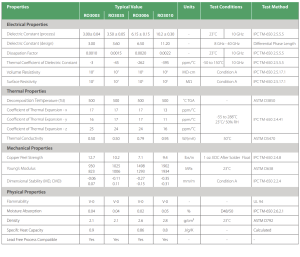
2. Rogers RO3006 Material Properties
| Property | Typical RO3006 value | Significance |
|---|---|---|
| Process dielectric constant | 6.15 ± 0.15 | Used primarily for material process control and comparison |
| Design dielectric constant | Approximately 6.4 | A more relevant starting value for certain circuit models |
| Dissipation factor | 0.002 at 10 GHz | Supports relatively low-loss high-frequency transmission |
| X-axis CTE | 17 ppm/°C | Close to the thermal expansion behavior of copper |
| Y-axis CTE | 17 ppm/°C | Supports in-plane dimensional stability |
| Z-axis CTE | 24 ppm/°C | Supports plated-through-hole thermal reliability |
| Thermal conductivity | 0.79 W/m·K | Higher than standard FR-4, but not a complete thermal solution |
| Moisture absorption | 0.02% | Helps limit moisture-related electrical variation |
| TCDk | Approximately −262 ppm/°C | Temperature-related Dk variation should be considered |
| Flammability rating | UL 94 V-0 | Supports applicable flame-retardancy requirements |
| Lead-free process compatibility | Yes | Compatible with lead-free assembly processes |
These are typical values released by Rogers Corporation. They shall not be treated as guaranteed specifications for all laminate thicknesses, copper foil types, production lots or test environments.
Designers shall refer to the latest manufacturer datasheet and verify the actual material stack-up with your PCB manufacturer.
3. Why Are the Process Dk and Design Dk Different?
The RO3006 datasheet lists two widely quoted dielectric constant values:
- Process Dk: 6.15 ± 0.15
- Design Dk: approximately 6.4
These two parameters have distinct use cases.
Process Dk is mainly adopted for material production control and standardized comparison. Design Dk is obtained via specific test fixtures and circuit structures, offering a more realistic baseline for practical circuit simulation.
The effective dielectric constant on a finished PCB circuit is further affected by the following factors:
- Microstrip or stripline stack-up
- Dielectric thickness
- Copper thickness
- Copper surface roughness
- Conductor width
- Etched conductor profile
- Solder mask coverage
- Operating frequency
- Multilayer bonding structure
- Test and extraction method
Designers therefore should not simply input 6.15 into every impedance calculator or RF simulation merely because RO3006 is the selected laminate.
It is critical to identify whether your calculation calls for Process Dk, Design Dk, or Effective Dk extracted from a representative circuit structure.
For devices highly sensitive to impedance, phase response or resonant frequency, prototype testing and correlation between the manufactured PCB and simulation model may still be required.
4. What Is the Advantage of the Higher Dk of RO3006?
RO3006 features a higher dielectric constant compared with RO3003, RO4003C and RO4350B.
A higher Dk shortens the effective wavelength of electromagnetic signals inside the dielectric substrate. For well-designed circuits, it enables size reduction for the following components:
- Microstrip transmission lines
- Stripline structures
- Filters
- Couplers
- Power dividers
- Matching networks
- Antenna elements
- Resonant circuits
This benefit is highly useful for RF modules with constrained PCB real estate.
Nevertheless, circuit miniaturization comes with manufacturing trade-offs.
With shrinking circuit geometries, conductor width, trace spacing, etching compensation, copper foil thickness and final fabrication tolerances become more stringent. Dimensional deviations that have minor impacts on large circuits will cause more prominent shifts in impedance, phase and resonant frequency for compact designs.
Therefore, the merit of RO3006 does not merely lie in the notion that “a higher Dk is better.”
A more precise summary:
For RF designs requiring defined electrical performance within a confined footprint, RO3006 delivers a favorable balance between circuit miniaturization and relatively low transmission loss.
5. Is RO3006 a Low-Loss Material?
RO3006 has a typical dissipation factor of roughly 0.002 at 10 GHz, classifying it as a low-loss high-frequency laminate.
Compared to standard FR-4, it is more suitable for circuits where insertion loss, signal attenuation, phase performance and high-frequency stability are critical metrics.
Nevertheless, insertion loss on a fabricated PCB cannot be determined solely by the datasheet Df value.
Other key contributing factors are listed below:
- Copper surface roughness
- Copper foil type
- Conductor length
- Operating frequency
- Dielectric thickness
- Conductor width
- Finished copper thickness
- Surface finish
- Conductor loss
- Dielectric loss
- Impedance discontinuities
- Via structures
- Connectors and transitions
At higher frequencies, conductor surface roughness contributes substantially to insertion loss. The real etched trace profile can also deviate from the ideal rectangular conductor assumed in simulation models.
Therefore, specifying only “Rogers RO3006” on a purchase order is insufficient.
For loss-critical designs, copper foil type, copper surface roughness, final copper thickness, transmission-line geometry and impedance specifications must also be clearly defined.
6. How Should the Thermal Properties of RO3006 Be Understood?
RO3006 features typical X, Y and Z-axis coefficients of thermal expansion (CTE) of approximately 17, 17 and 24 ppm/°C respectively.
These CTE values are reasonably matched to copper’s thermal expansion characteristics. Specifically, the low Z-axis CTE minimizes expansion mismatch between the dielectric substrate and plated barrel during thermal cycling.
This property enhances plated-through-hole (PTH) reliability.
RO3006 delivers a typical thermal conductivity of 0.79 W/m·K, superior to standard FR-4. This benefit suits applications like RF power amplifiers, where heat must be dissipated from active devices.
Nevertheless, the 0.79 W/m·K thermal conductivity does not imply the laminate by itself can resolve all thermal management challenges.
A robust thermal design may additionally require:
- Suitable copper coverage
- Thicker copper
- Ground planes
- Thermal vias
- Metal baseplates
- Thermal interface materials
- Heatsinks
- Controlled airflow
- Proper component placement
- Appropriate enclosure design
It is also critical not to confuse low CTE and enhanced thermal conductivity with dielectric stability across temperature.
RO3006 features a typical thermal coefficient of dielectric constant (TCDk) of approximately −262 ppm/°C. This indicates temperature-induced shifts in dielectric performance must be assessed for applications highly sensitive to phase drift or resonant-frequency variation.
This distinction is often overlooked when a material is loosely labelled “thermally stable.”
RO3006 delivers favorable thermomechanical properties; nevertheless, its electrical performance versus temperature must be taken into account throughout the design phase.
7. Moisture Absorption and Environmental Performance
RO3006 features a typical moisture absorption rate of approximately 0.02%.
Low moisture absorption minimizes water’s impact on high-frequency electrical performance, bringing advantages for applications including:
- Outdoor communication equipment
- Antenna systems
- Automotive electronics
- RF products used in humid environments
- Long-term wireless infrastructure installations
Nevertheless, low laminate moisture absorption does not render the full PCB immune to environmental effects.
Finished-board reliability also depends on:
- Solder mask coverage
- Board-edge protection
- Via construction
- Surface cleanliness
- Ionic contamination
- Surface finish
- Assembly residues
- Conformal coating
- Enclosure protection
Material performance constitutes a key element of environmental reliability, yet it alone cannot deliver a full solution.
8. Common RO3006 Applications
Rogers Corporation defines multiple application fields for RO3006 and the RO3000 material series.
8.1 Antenna Systems
RO3006’s higher Dk enables size reduction for selected antenna and feed structures. Its low dissipation factor also keeps signal loss under control.
Final antenna performance is determined by circuit geometry, copper properties, dielectric thickness, ground plane structure, manufacturing tolerances and operating environmental conditions.
8.2 Communication Systems
RO3006 is suitable for RF front-ends, microwave communication modules, and other circuits that demand controlled impedance, relatively low insertion loss and compact form factors.
8.3 Backhaul Radios
For microwave backhaul and associated communication hardware, well-controlled dielectric characteristics and low transmission loss preserve signal integrity.
8.4 RF Power Amplifiers
The combination of low loss, superior thermal conductivity versus FR-4, and low Z-axis CTE renders RO3006 a candidate for selected RF power amplifier circuits.
A full thermal design must incorporate adequate copper areas, thermal vias, baseplates and external heat dissipation structures.
8.5 Active-Safety and Radar-Related Electronics
RO3006 can be evaluated for specific active safety and radar circuits. Nevertheless, it is not a default choice for all 77 GHz or 79 GHz automotive radar designs.
Material selection for mmWave radar shall also take the following factors into account:
- Actual loss at the operating frequency
- Dk tolerance
- Dielectric-thickness tolerance
- Copper-foil roughness
- Phase consistency
- Antenna architecture
- Fabrication capability
- Production-lot consistency
Other materials such as RO3003G2 feature properties specially optimized for 77/79 GHz automotive radar designs.
Material selection shall be based on actual circuit architecture and performance requirements instead of application category alone.
9. RO3006 vs. RO3003, RO3010 and RO4350B
| Property | RO3003 | RO3006 | RO3010 | RO4350B |
|---|---|---|---|---|
| Material system | Ceramic-filled PTFE | Ceramic-filled PTFE | Ceramic-filled PTFE | Ceramic-filled hydrocarbon |
| Process Dk | 3.00 ± 0.04 | 6.15 ± 0.15 | 10.20 ± 0.30 | Approximately 3.48 ± 0.05 |
| Design Dk | Approximately 3.16 | Approximately 6.4 | Approximately 11.2 | Approximately 3.66 |
| Typical Df | Approximately 0.0010 | Approximately 0.0020 | Approximately 0.0022 | Approximately 0.0037 |
| Main characteristic | Low Dk and very low loss | Higher Dk with compact circuit potential | Very high Dk for greater miniaturization | Easier high-volume fabrication |
| Processing family | Specialized PTFE processing | Specialized PTFE processing | Specialized PTFE processing | Thermoset processing |
| Typical selection consideration | Antennas and low-loss circuits | Size and loss balance | Strong miniaturization requirement | Fabrication convenience and production cost |
RO3003 is a candidate where low Dk and ultra-low loss are prioritized.
RO3006 suits applications requiring higher Dk for circuit size reduction while keeping relatively low loss.
RO3010 delivers an even higher Dk with greater miniaturization capability. That said, compact conductors, impedance control and manufacturing tolerances become more critical.
RO4350B is preferred for high-volume production ease and processing compatibility similar to standard FR-4.
Material replacement shall not be made merely based on similar nominal Dk or Df figures.
Even for laminates with matching dielectric characteristics, differences may exist in:
- Resin system
- Glass reinforcement
- Copper options
- Thickness tolerance
- Thermal behavior
- Fabrication method
- Bonding requirements
- Mechanical stability
Accordingly, any material substitution must be reviewed jointly by design engineer, PCB fabricator and material supplier where applicable.
10. Why Can’t RO3006 Be Processed Exactly Like FR-4?
RO3006 is a ceramic-filled PTFE laminate. It differs from standard FR-4 and thermoset high-frequency materials like RO4350B.
It is available for double-sided and multilayer PCB designs, yet the PCB fabricator must possess sufficient experience processing PTFE-based high-frequency substrates.
Key manufacturing considerations are listed below.
10.1 Material Handling
Non-woven glass reinforced PTFE laminates exhibit mechanical characteristics distinct from rigid FR-4.
Material handling throughout cutting, drilling, imaging, registration, lamination and shipment shall be carefully managed to prevent stretching, bending, surface defects and dimensional drift.
For constructions demanding higher rigidity and tighter registration control, woven-glass-reinforced options within the RO3200 product family can be considered.
10.2 Drilling Parameters
Drilling conditions, feed rate, spindle speed, entry sheet, backup sheet, stack height and tool life all impact hole quality.
Improper drilling parameters may cause the following defects:
- Hole-wall smearing
- Burrs
- Distorted hole entries
- Rough hole walls
- Contamination
- Poor subsequent metallization
The drilling recipe shall be customized for the laminate construction instead of directly adopting standard FR-4 drilling procedures.
10.3 Hole-Wall Preparation
PTFE features inherently low surface energy. Standard FR-4 desmear treatment alone cannot generate a proper surface to ensure reliable electroless copper bonding.
Subject to production workflow and board stack-up, plasma treatment or qualified chemical sodium etching can be applied to condition PTFE hole walls prior to metallization.
Inadequate hole-wall preparation may lead to:
- Incomplete electroless copper coverage
- Weak copper-to-hole-wall adhesion
- Voids in the plated hole
- Failure after thermal shock
- Intermittent open circuits during long-term use
Rogers indicates plasma-conditioned hole surfaces are more fragile than chemically treated surfaces and require careful handling in downstream processes.
10.4 Etching Compensation
Thanks to RO3006’s higher Dk enabling miniaturized RF circuit structures, certain designs feature narrow or dimension-critical transmission lines.
Minor variations in conductor width, final copper thickness and etched sidewall profile will impact impedance and electrical length.
The PCB fabricator shall implement proper engineering compensation based on copper weight, circuit geometry and etching capacity.
10.5 Multilayer Bonding
Standard FR-4 prepreg shall not be used by default for RO3006 multilayer stack-ups.
Bonding material selection shall consider the following criteria:
- Electrical performance
- Lamination temperature
- Resin flow
- Required dielectric thickness
- Copper treatment
- Adhesion requirements
- Finished reliability
Where RO3006 is laminated together with FR-4, RO4350B or other laminates within a hybrid multilayer PCB, the manufacturer shall additionally assess:
- Lamination compatibility
- X- and Y-axis dimensional movement
- Z-axis expansion
- Resin-flow behavior
- Layer-to-layer registration
- Bond strength
- Finished impedance
- Bow and twist
All hybrid high-frequency stack-ups shall be reviewed prior to design release for manufacturing.
11. Critical Quality Controls for RO3006 PCB Manufacturing
Merely verifying the laminate brand cannot guarantee reliable RO3006 PCBs.
Full manufacturing process controls are required.
11.1 Material Verification
The manufacturer shall verify the below items:
- Material type
- Laminate thickness
- Copper weight
- Copper foil type
- Production lot
- Material source
- Storage and handling condition
This avoids using visually similar substrates with divergent electrical performance.
11.2 Engineering Compensation
Conductor compensation shall take into account final copper thickness, line density, dielectric thickness, impedance targets and etching capacity.
11.3 Drilling Quality
Hole entry profile, hole-wall condition, smear, burrs and tool wear shall be monitored. Drilling parameters and tool life limits shall be defined for the actual PTFE stack-up.
11.4 Hole-Wall Treatment
Plasma or chemical treatment shall generate a qualified, consistent surface for subsequent electroless copper deposition.
11.5 Circuit Imaging
High-Dk designs often feature compact, dimension-critical RF traces.
Laser Direct Imaging (LDI) minimizes film-induced dimensional deviation and delivers better control over conductor placement & imaging compensation.
Nevertheless, LDI alone cannot guarantee RF performance. Etching control and final conductor dimension measurement are equally critical.
11.6 Copper Plating and PTH Quality
The fabricator shall control electroless copper coverage, final plated copper thickness inside holes, plating uniformity and hole-wall integrity.
Microsection analysis can be performed to assess the finished plated-through-hole (PTH) structure as needed.
11.7 Impedance Control
Final impedance performance is determined by more than just the nominal trace width.
Other influencing factors are listed below:
- Actual dielectric thickness
- Effective Dk
- Copper thickness
- Etched conductor profile
- Copper roughness
- Solder mask
- Reference-plane structure
The full stack-up shall be validated prior to production. Impedance test coupons shall be measured if specified in the specs.
11.8 Final Verification
Subject to product specifications, inspection items may cover:
- Electrical testing
- Controlled-impedance testing
- Microsection analysis
- Dimensional inspection
- Visual inspection
- Hole-copper measurement
- Surface-finish inspection
For circuits requiring stringent RF performance, customers shall also conduct application-level RF testing on the finished design.
12. Information Required for an RO3006 PCB Quotation
To enable accurate quotation and DFM review, the following information shall be provided:
- Gerber or ODB++ data
- PCB layer count
- Finished board thickness
- RO3006 core thickness
- Copper thickness
- Copper foil requirement
- Complete stack-up
- Controlled-impedance structures
- Target impedance values
- Impedance tolerance
- Operating frequency
- Identification of critical RF traces
- Surface finish
- Minimum line width and spacing
- Minimum finished hole size
- Hole-copper requirement
- Board-outline tolerance
- Testing requirements
- Prototype and production quantities
- Required delivery date
If the stack-up is not finalized yet, customers may first supply the required layer count, finished board thickness, impedance target, operating frequency and preferred material.
Our PCB engineering team will assess available laminate thickness options and propose a manufacturable stack-up for your confirmation.
13. RO3006 PCB Manufacturing Support from SQPCB
SQPCB offers prototype and mass production services for Rogers, RF, microwave and other high-frequency PCB projects.
Prior to production release, our engineering team will conduct review covering:
- RO3006 material and thickness selection
- Double-sided or multilayer construction
- Hybrid stack-up manufacturability
- Controlled-impedance structures
- High-frequency conductor dimensions
- Drilling and hole-wall preparation
- Copper thickness
- Surface finish
- Board-edge requirements
- Dimensional tolerances
- Testing and acceptance criteria
We adopt LDI for circuit and solder mask imaging to enhance registration accuracy and compensation control. Drilling, hole-wall treatment, electroless copper deposition, electroplating, circuit patterning, solder mask application and electrical test will be scheduled based on the actual material and board structure.
During the material selection phase, RO3006 shall be evaluated alongside RO3003, RO3010, RO4350B and other Rogers PCB materials, instead of being selected based on a single parameter only.
For complex stack-up structures, material selection shall also be assessed in conjunction with our multilayer PCB manufacturing capabilities, icovering lamination, layer alignment, impedance control and plated via reliability.
For projects needing rapid design verification, customers may take advantage of our quick-turn PCB manufacturing service and submit Gerber data, stack-up details and impedance specs for DFM review.
14. Conclusion
Rogers RO3006 is a high-Dk, low-loss, ceramic-filled PTFE circuit laminate.
Its key features are listed below:
- Process Dk of 6.15 ± 0.15
- Potential reduction of certain RF circuit dimensions
- Typical Df of approximately 0.002 at 10 GHz
- Low X-, Y-, and Z-axis CTE values
- Thermal conductivity higher than standard FR-4
- Typical moisture absorption of 0.02%
- Suitability for double-sided and multilayer high-frequency circuits
Nevertheless, RO3006 cannot be fabricated in the same way as conventional FR-4.
Strict process controls are required for material handling, drilling, hole-wall treatment, copper deposition, conductor compensation, lamination and controlled impedance
TCDk must also be assessed for RF circuits sensitive to temperature-induced phase shift or resonant frequency drift.
Hence, RO3006 shall not be chosen merely for its “high Dk” and “low loss”. The critical factor is whether its material characteristics align with the project’s operating frequency, circuit geometry, temperature range, stack-up structure, reliability specs and manufacturing constraints.
Proper material selection together with mature PCB fabrication and tight process control transforms datasheet material properties into consistent, reliable performance of the final boards.
Submit your Gerber data, stack-up information and impedance requirements to SQPCB for DFM and manufacturability evaluation.
15. Frequently Asked Questions About Rogers RO3006
1. Are Rogers 3006 and RO3006 the same material?
Yes. “Rogers 3006” is a widely used shorthand for the Rogers RO3006™ high-frequency laminate. Its official product designation is RO3006 laminate.
2. Should I use 6.15 or 6.4 as the dielectric constant of RO3006?
6.15 ± 0.15 is the published Process Dk, while roughly 6.4 refers to Design Dk. The correct value for simulation varies with circuit topology, operating frequency, copper foil properties and simulation modeling approach. Designers cannot simply apply 6.15 for all calculations.
3. Is RO3006 suitable for 77 GHz automotive radar?
RO3006 is applicable for high-frequency and some radar circuits. However, its compatibility for 77 GHz /79 GHz automotive radar designs needs assessment based on insertion loss, Dk tolerance, copper roughness, phase stability, antenna architecture and manufacturing constraints. Operating frequency alone is not enough for material selection.
4. Can RO3006 be used in a multilayer PCB?
Yes. RO3006 works for double-sided and multilayer high-frequency circuits. Proper bonding film and stack-up structure must be chosen. For hybrid constructions mixing RO3006 with FR-4 or other Rogers laminates, it is necessary to verify lamination compatibility, dimensional shift, impedance performance, and board bow & twist.
5. Can RO3006 be processed using a standard FR-4 process?
Not fully. RO3006 is a ceramic-filled PTFE laminate and demands dedicated process control for drilling, hole-wall activation, electroless copper deposition, material handling, etching compensation and lamination. Fabrication should be performed by a PCB vendor with proven experience in PTFE high-frequency substrates.
RO3006™, RO3000®, RO3003™, RO3010™, RO3003G2™, RO3200™, RO4003C™ and RO4350B™ are trademarks of Rogers Corporation. SQPCB is an independent PCB manufacturer and has no affiliation with Rogers Corporation..

- Special PCB
- long board pcb
- Flexible PCBs
- Special PCB
- Express Printed Circuit Board
- Pcb Prototype
- LED PCB
- PCB
- Pcb Meaning
- Printed Circuit Board
- Pcb manufacturer
- Rigid pcb board
 Quote
 E-mail