Introduction to PCB Profiling
In the ever-evolving world of electronics manufacturing, PCB profiling plays a pivotal role in ensuring quality, reliability, and efficiency. As the demand for more complex and compact electronic devices grows, the importance of precise profiling techniques has become increasingly crucial. This introduction delves into the fundamentals of PCB profiling, highlighting its significance, key methodologies, and the technological advancements that are shaping the future of the industry.
Profiling, the systematic measurement and optimization of critical process parameters, is a cornerstone of modern printed circuit board (PCB) manufacturing. By analyzing and controlling variables such as temperature, chemical concentrations, and mechanical forces, profiling ensures consistent quality, reduces defects, and enhances yield. This guide explores the role of profiling across PCB fabrication stages, from material preparation to final testing, and highlights emerging technologies reshaping this vital practice.
PCB Profiling
The Essence of PCB Profiling
PCB profiling refers to the systematic process of monitoring and analyzing the thermal, electrical, and mechanical characteristics of printed circuit boards during manufacturing. It serves as a critical quality control measure, allowing manufacturers to detect defects, optimize processes, and enhance product performance.
- Thermal Profiling ensures that the soldering process adheres to the specified temperature curves.
- Electrical Profiling verifies signal integrity, impedance matching, and current flow.
- Mechanical Profiling monitors the structural stability of the board, preventing warpage and stress-related failures.
The Importance of PCB Profiling in Modern Electronics
With the rapid advancement of technologies such as 5G, IoT, and AI-driven devices, the complexity of PCB designs has increased exponentially. Profiling has become indispensable in:
- Ensuring Solder Joint Quality: By analyzing temperature distribution during reflow soldering, manufacturers can prevent cold joints and overheating.
- Enhancing Signal Integrity: Electrical profiling helps mitigate issues like crosstalk and electromagnetic interference.
- Preventing Mechanical Stress: Mechanical profiling detects potential warping and bending, ensuring structural integrity.
Key Components of PCB Profiling
- Data Acquisition Systems: Advanced sensors and thermal cameras capture real-time data.
- Software Analytics Tools: AI-driven platforms analyze data patterns and provide actionable insights.
- Feedback Mechanisms: Automated systems adjust process parameters to maintain optimal conditions.
Evolution of PCB Profiling Techniques
The evolution of PCB profiling has been driven by technological innovations and industry demands:
- Traditional Methods: Manual inspection and basic thermal mapping.
- Modern Approaches: AI-powered predictive analytics and IoT-enabled monitoring systems.
- Future Trends: Integration of machine learning algorithms and advanced robotics for precision control.
Challenges in PCB Profiling
Despite its benefits, PCB profiling faces several challenges:
- Complex Multi-Layer Designs: Managing heat distribution across multiple layers is challenging.
- Miniaturization of Components: Smaller components require higher precision and accuracy.
- Environmental Variables: Temperature and humidity fluctuations can impact performance.
The Role of PCB Profiling in Various Industries
- Automotive Electronics: Ensuring the reliability of engine control units and safety systems.
- Consumer Electronics: Enhancing the performance of smartphones, laptops, and wearables.
- Medical Devices: Maintaining the accuracy and functionality of life-saving equipment.
- Aerospace and Defense: Guaranteeing the durability and reliability of mission-critical systems.
PCB profiling involves capturing detailed thermal, electrical, and mechanical data to optimize the assembly process. It is essential for reducing defects, ensuring product reliability, and enhancing manufacturing efficiency.
Profiling in Key PCB Manufacturing Processes
Thermal Profiling in Reflow Soldering
Reflow soldering, a critical step in surface mount technology (SMT), relies on precise thermal profiling to achieve reliable solder joints.
- Temperature Zones: Preheat, soak, reflow, and cooling phases must follow a strict profile.
- Challenges: Variations in component sizes and PCB thickness affect heat distribution.
- Solutions: Multi-zone ovens with real-time thermocouple feedback.
Chemical Profiling in Etching and Plating
Accurate profiling of chemical baths ensures uniform etching and plating results.
- Etchant Concentration Profiling: Monitors and adjusts acidic/alkaline solutions to maintain consistent copper removal rates.
- Electroplating Profiling: Controls current density, pH, and temperature for even metal deposition.
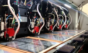
Mechanical Profiling in Drilling and Routing
- Drill Speed and Feed Rate Profiling: Optimizes hole quality in materials like FR-4, Rogers, and metal-core PCBs.
- Tool Wear Monitoring: Predictive algorithms adjust parameters as drill bits degrade.
3. Advanced Profiling Techniques and Technologies
Real-Time Data Acquisition Systems
- IoT Sensors: Embedded sensors in equipment collect temperature, pressure, and chemical data.
- Edge Computing: On-site processing reduces latency for immediate parameter adjustments.
Machine Learning-Driven Profiling
- Predictive Analytics: AI models forecast optimal parameters based on historical data.
- Anomaly Detection: Flags deviations (e.g., temperature spikes) before defects occur.
3D Profiling for High-Density Interconnect (HDI) PCBs
- Laser Profiling: Measures microvia depth and diameter with sub-micron accuracy.
- X-Ray Profiling: Inspects buried vias and layer alignment in multilayer boards.
Thermal Profiling: The Heart of PCB Manufacturing
-
Reflow Soldering Profiling:
- Monitors the heat distribution during the soldering process.
- Prevents cold solder joints and overheating of sensitive components.
-
Wave Soldering Profiling:
- Tracks temperature flow through molten solder waves.
- Essential for through-hole component assembly.
-
Selective Soldering Profiling:
- Focuses on specific areas of the board.
- Reduces thermal stress on heat-sensitive components.
Electrical Profiling: Ensuring Circuit Integrity
- Current Flow Analysis: Monitors resistance and voltage levels.
- Impedance Matching: Essential for high-speed and RF circuits.
- Signal Integrity Testing: Identifies crosstalk and electromagnetic interference.
Mechanical Profiling: Preventing Warpage and Stress
- Board Flex Monitoring: Detects mechanical stress and bending.
- Material Expansion Analysis: Ensures compatibility between copper and substrate materials.
- Vibration Testing: Verifies durability in harsh environments.
Advanced Equipment for PCB Profiling
- KIC Profiler: Tracks real-time temperature data.
- ECD Oven Rider: Monitors reflow oven performance.
- FLIR Thermal Cameras: Visualizes heat distribution.
Training and Skill Development for Effective PCB Profiling
Investing in workforce training is crucial for successful PCB profiling implementation:
- Operator Certification Programs: Ensuring that technicians are well-versed in operating profiling equipment and interpreting data.
- Continuous Learning Initiatives: Keeping up with new profiling technologies and industry standards.
- Collaboration with R&D Teams: Integrating feedback from design engineers to optimize profiling strategies for new product designs.
Regulatory Compliance and Quality Standards
Compliance with international standards is critical for global market acceptance:
- IPC-610 and IPC-6012 Standards: Governing PCB quality and performance.
- ISO 9001 and ISO 13485 Certifications: Ensuring quality management systems for industrial and medical electronics.
- RoHS and REACH Directives: Adhering to environmental regulations for hazardous substances.
Data Analysis and Process Optimization
-
Data Logging and Analysis:
- Captures temperature curves and electrical performance data.
- Helps identify process inefficiencies.
-
Feedback Loop Integration:
- Automated systems adjust soldering parameters based on real-time data.
-
Machine Learning Algorithms:
- Predict potential defects and suggest corrective actions.
Case Study: Automotive PCB Manufacturing
- Objective: Improve solder joint reliability for engine control units.
- Solution: Implement advanced thermal profiling tools.
- Result: 30% reduction in defect rates and enhanced product lifespan.
Future Trends in PCB Profiling
-
IoT-Integrated Profiling Systems:
- Real-time monitoring and remote control.
-
AI-Powered Predictive Analytics:
- Machine learning algorithms for defect prediction.
-
Sustainable Profiling Practices:
- Energy-efficient ovens and eco-friendly materials.
Conclusion: The Future of PCB Profiling
As the electronics industry advances, PCB profiling remains a cornerstone for ensuring quality, reliability, and performance in printed circuit boards. The continuous evolution of technology, coupled with increasing complexity in design and manufacturing processes, makes profiling an indispensable practice for manufacturers aiming to meet the demands of modern applications.
1. Enhanced Quality Control
PCB profiling has proven to be instrumental in:
- Minimizing Defects: By identifying thermal anomalies, solder joint inconsistencies, and mechanical stress points, profiling reduces the risk of defective boards reaching the market.
- Improving Yield Rates: With accurate data and real-time feedback, manufacturers can optimize production parameters and reduce waste.
- Enhancing Reliability: Profiling ensures the longevity and durability of PCBs, particularly in high-stress environments like automotive, aerospace, and medical devices.
2. Technological Innovations Driving PCB Profiling
The integration of cutting-edge technologies is transforming PCB profiling:
- AI and Machine Learning Algorithms: Predictive analytics can identify potential failure points before they occur, allowing for proactive adjustments.
- IoT-enabled Monitoring Systems: Real-time data collection and analysis help manufacturers respond to process variations instantly.
- Advanced Sensors and Imaging Tools: High-resolution thermal cameras and laser scanners provide precise data for in-depth analysis.
3. Overcoming Industry Challenges
Despite the advancements, PCB profiling faces several challenges:
- Managing Multi-Layered Boards: Ensuring consistent heat distribution and signal integrity across multiple layers requires sophisticated techniques.
- Addressing Miniaturization Trends: As components shrink, the need for higher precision and accuracy becomes critical.
- Environmental Factors: External variables such as temperature fluctuations and humidity can impact PCB performance, necessitating adaptive profiling strategies.
4. Future Prospects of PCB Profiling
Looking ahead, the future of PCB profiling is promising:
- Automated and Self-Optimizing Systems: AI-driven feedback loops will enable automatic adjustments to process parameters.
- Cloud-Based Data Analysis: Centralized platforms will allow for remote monitoring and data sharing across global manufacturing facilities.
- Sustainability and Energy Efficiency: Optimized profiling can reduce energy consumption and minimize material waste, contributing to greener manufacturing practices.
5. The Role of PCB Profiling in Industry 4.0
In the era of smart manufacturing, PCB profiling will play a critical role in:
- Predictive Maintenance: Identifying wear and tear on production equipment before failures occur.
- Enhanced Traceability: Tracking quality data throughout the production process for compliance and accountability.
- Customized Solutions: Tailoring profiling strategies to specific applications and customer requirements.
Final Thoughts
PCB profiling is not merely a quality control measure but a strategic asset that drives innovation, efficiency, and customer satisfaction. By embracing emerging technologies and addressing industry challenges, manufacturers can leverage profiling to stay competitive in an increasingly demanding market.

- long board pcb
- Flexible PCBs
- Special PCB
- Express Printed Circuit Board
- Pcb Prototype
- LED PCB
- PCB
- Printed Circuit Board
- Pcb meaning
- Pcb manufacturer
- Rigid pcb board
- Rigid Flex PCB
 Quote
Quote
 E-mail