Introduction
In PCB manufacturing, drilling is often viewed as a basic mechanical process: create holes according to the drill file and move to the next production stage. In reality, the condition of the drilled hole wall can have a major influence on subsequent desmear, electroless copper, electroplating, reliability testing, and final production yield.
A hole can meet its diameter and positional requirements while still having a problematic internal surface. This is why hole wall quality deserves attention, particularly for multilayer PCBs, high-density designs, and boards where plated-through-hole reliability is critical. IPC guidance emphasizes that a properly drilled hole should have a smooth wall and be free from conditions such as delamination, burning, crushed insulation, and protruding fibers. Poor drilling can contribute to rough plating, plating voids, thin copper, cracks, and other downstream defects.
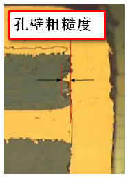
Hole Wall Roughness
What Is Hole Wall Roughness?
Hole wall roughness refers to microscopic or visible irregularities on the internal surface of a drilled PCB hole. Instead of having a relatively uniform wall, the surface may contain resin tear-out, exposed or protruding glass fibers, pits, scratches, smeared resin, or other local surface defects.
The condition is strongly influenced by the interaction between the drill and the laminate. A PCB laminate contains resin and reinforcing glass fibers with different mechanical properties. During drilling, excessive heat, unsuitable feed rates, excessive drilling speed, worn tools, or inappropriate drilling parameters can cause the resin to smear while glass fibers may be torn or pulled from the surrounding material.
Drill wear is particularly important. Research on PCB drilling has shown that increasing drill wear can deteriorate inner-wall quality, while margin wear can increase glass-fiber fraying and contribute to greater wall roughness.
Importantly, surface roughness is not the same as hole diameter tolerance. A hole may have the correct finished diameter but still present an inconsistent surface for subsequent copper deposition.
Why Hole Wall Roughness Matters for PCB Plating
Copper plating depends on a properly prepared hole surface. After drilling, desmear and hole-conditioning processes must remove unwanted resin residues and prepare the surface for metallization. Electroless copper then establishes the initial conductive layer before additional copper is built up through electroplating.
When the drilled wall is excessively irregular, the plating process has to cover a more complicated surface. Deep recesses, torn glass fibers, resin smear, and localized defects can make copper deposition less uniform. IPC documentation identifies poor drilling as a potential contributor to rough plating, nodules, plating voids, thin plating, plating cracks, and skip plating.
This creates an important manufacturing principle: plating quality cannot be separated from drilling quality. Improving the plating bath alone may not solve a defect that actually originates from the hole wall.
Hole Wall Roughness: Cost Factors and PCB Performance Impact
The cost of poor hole-wall quality is not limited to the drilling operation itself. A factory may need additional drill changes, tighter process monitoring, extra desmear control, additional inspection, cross-section analysis, rework, or even complete panel scrapping.
For high-volume production, even a relatively small defect rate can become expensive because one panel contains many drilled holes. If a problem is discovered only after copper plating or electrical testing, the material and processing costs accumulated before detection are much higher.
| Factor | Potential Impact |
|---|---|
| Drill wear | More frequent tool replacement and process instability |
| Incorrect drilling parameters | Rough walls, glass-fiber damage, resin smear |
| Poor desmear control | Weak copper adhesion or incomplete metallization |
| Uneven plating | Reduced effective copper thickness and reliability risk |
| Excessive defects | Rework, scrap, and lower production yield |
| Difficult inspection | Additional cross-section and process-analysis costs |
From a performance perspective, the most important concern is long-term interconnection reliability. Rough or damaged hole walls can contribute to nonuniform plating and localized weak points. Under thermal cycling, mechanical stress, or repeated assembly processes, these weaknesses can become more significant. Research presented by IPC has also linked drilling and plating conditions with plated-through-hole reliability and observed that greater wall roughness can be associated with plating folds and locally low copper thickness.
Hole Wall Roughness: Common Production Problems and Solutions
Several production conditions can increase wall roughness. Worn drills are a common source because the cutting edge no longer removes laminate material cleanly. Excessive feed rate can increase mechanical stress and damage glass bundles, while unsuitable spindle speed can contribute to heat generation and resin deformation.
Material construction also matters. Different resin systems, glass styles, copper structures, and laminate thicknesses respond differently during drilling. Therefore, simply applying one drilling parameter set to every PCB material is unlikely to provide consistent results.
A practical control strategy should include tool-life management, optimized spindle speed and feed rate, appropriate entry and backup materials, correct stack-up selection, and regular cross-sectional inspection. The desmear process should also be carefully controlled: insufficient treatment can leave resin residues, while overly aggressive treatment can unnecessarily alter the dielectric structure.
When a plating defect appears, engineers should therefore trace the process backward instead of immediately adjusting the plating chemistry. Checking drill wear, drilling parameters, hole-wall appearance, resin smear, glass-fiber condition, and desmear effectiveness can help identify the real root cause. IPC troubleshooting guidance similarly connects drilling-related conditions with downstream plating and hole-quality problems.
Hole Wall Roughness: How Manufacturers Can Improve Yield
The best approach is to treat hole-wall quality as a process-control issue rather than an inspection-only issue. By the time severe roughness becomes visible through plating defects or reliability failures, the production cost has already increased.
Manufacturers should monitor drill life according to actual hole count and material conditions, rather than relying only on a fixed replacement schedule. Drilling parameters should be validated for each laminate construction, and first-article or periodic cross-section analysis can help verify whether the process is producing consistent walls.
It is also valuable to connect drilling data with plating and electrical-test results. If plating defects repeatedly appear on specific materials, tool-life stages, or drilling programs, the correlation can reveal process weaknesses that ordinary final inspection may miss.
In my view, this is where hole-wall control becomes particularly valuable: a smooth hole wall is not simply an aesthetic requirement; it is part of the foundation for reliable metallization. Controlling the surface before plating is generally more efficient than trying to compensate for an unstable surface later in the manufacturing process.
Conclusion
Hole-wall condition is an easily overlooked part of PCB manufacturing because it is hidden inside the board. However, this hidden surface directly participates in the metallization process and can influence plating uniformity, hole reliability, manufacturing yield, and overall production cost.
For standard boards, minor surface irregularities may not necessarily create a functional problem when the finished hole still satisfies applicable requirements. However, as PCB designs become denser and reliability requirements become more demanding, process margins become narrower. A defect that appears insignificant during drilling can become much more important after desmear, copper deposition, thermal cycling, and assembly.
The practical lesson is simple: do not evaluate a drilled hole only by its diameter and position. The condition of its internal wall also deserves attention. Effective tool management, optimized drilling parameters, controlled desmear, appropriate inspection, and close cooperation between drilling and plating processes can reduce hidden defects before they become expensive failures.
For PCB manufacturers and buyers, discussing hole-wall quality early in the engineering process can therefore help improve consistency, reduce unnecessary rework and scrap, and build a more reliable manufacturing process from the inside out.
FAQs
1. What causes rough PCB hole walls?
Common causes include worn drill bits, inappropriate spindle speed or feed rate, excessive drilling heat, unsuitable drilling parameters, improper stack-up conditions, and differences in laminate construction. Glass-fiber tearing and resin deformation can both contribute to an irregular wall.
2. How does roughness affect PCB plating?
An irregular hole wall can make surface preparation and copper deposition less consistent. Severe defects may contribute to rough plating, thin copper areas, plating voids, or weak adhesion, depending on the specific process conditions.

- Special PCB
- long board pcb
- Flexible PCBs
- Special PCB
- Express Printed Circuit Board
- Pcb Prototype
- LED PCB
- PCB
- Pcb Meaning
- Printed Circuit Board
- Pcb manufacturer
- Rigid pcb board
 Quote
 E-mail