Introduction
Printed Circuit Boards (PCBs) are fundamental to the modern electronics industry, as they provide the electrical connections for virtually all electronic devices. As such, the quality and reliability of PCBs are paramount. One factor that plays a significant role in the overall quality of a PCB is hole wall roughness. In PCB manufacturing, vias are created in the substrate to allow electrical signals to pass between different layers of the board. The quality of these vias—specifically the roughness of their walls—can significantly impact the final performance and reliability of the PCB.
This blog post will explore the effect of hole wall roughness on PCB quality, its causes, and how to control it in the manufacturing process. Understanding the relationship between hole wall roughness and PCB performance is essential for ensuring that your PCBs meet the required standards for high-speed signal transmission, longevity, and mechanical robustness.
1. What is Hole Wall Roughness in PCB Manufacturing?
In PCB manufacturing, vias are holes that are drilled or laser-cut into the board to facilitate electrical connections between layers. These vias are then plated with copper to form electrical pathways. The hole wall roughness refers to the microscopic texture and irregularities on the inner surfaces of these vias after the drilling or laser process.
The roughness can result from several factors, including the type of drill bit or laser used, the speed and pressure during drilling, and the material properties of the PCB itself. The rougher the hole wall, the more likely it is to affect the electrical performance, mechanical strength, and longevity of the PCB.
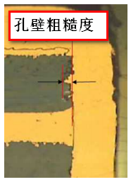
Hole Wall Roughness
2. Causes of Hole Wall Roughness
The primary causes of hole wall roughness can be categorized into material factors, drilling techniques, and post-drilling processes:
A. Drilling Techniques
-
Drill Bit Quality and Type: The type and condition of the drill bit used in the PCB manufacturing process significantly impact the quality of the hole walls. A worn-out drill bit, for instance, can lead to uneven hole walls. Using improper drill bits for certain PCB materials, such as those with a high glass transition temperature, can also result in rougher surfaces.
-
Drilling Speed and Feed Rate: The drilling speed and feed rate must be optimized to ensure smooth drilling. High speeds or excessive feed rates can generate heat, leading to thermal degradation of the PCB material and rougher hole walls. Conversely, too slow a speed can result in poor hole formation and increased material drag, also affecting the hole surface quality.
-
Laser Drilling: In some cases, laser drilling is used for high-precision or high-density PCBs. While laser drilling can create smooth holes, improper laser parameters, such as excessive power or incorrect pulse duration, can cause irregular hole walls and surface damage.
B. Material Factors
-
PCB Material Composition: Different PCB materials have varying properties that can affect hole wall roughness. For instance, FR4, a common PCB material, can have different hole wall textures depending on the resin-to-glass ratio and the specific manufacturing process. Harder materials, such as ceramics or high-frequency laminates, may produce more roughness when drilled due to their higher hardness.
-
Surface Treatment: In some cases, the surface treatment applied to the PCB material prior to drilling—such as etching or coating—can impact the smoothness of the hole walls. If the surface treatment isn’t uniform, it can cause uneven drilling, which results in more roughness.
C. Post-Drilling Processes
-
Plating Process: After drilling, the vias are typically plated with copper to form electrical connections. The plating process can contribute to hole wall roughness if not executed correctly. Poor plating can result in voids or irregularities on the hole surface, compromising the overall quality of the PCB.
-
Cleaning: After drilling and plating, the vias must be cleaned thoroughly. Any residual material left in the holes or on the hole walls can contribute to roughness. Chemical etching or laser cleaning techniques are often employed to remove debris and smooth the hole walls, but improper cleaning can lead to a rough surface finish.
3. How Hole Wall Roughness Affects PCB Quality
Hole wall roughness may seem like a minor issue, but it can have a profound impact on the overall performance, reliability, and manufacturability of a PCB. Below are the key areas where hole wall roughness can cause problems:
A. Electrical Performance
-
Signal Integrity: High-frequency signals are particularly sensitive to imperfections in the PCB. Irregularities in the hole walls can lead to signal reflection, cross-talk, and increased inductance. These factors can degrade the quality of signal transmission, especially in high-speed and high-frequency circuits.
-
Increased Resistance: Rough hole walls can lead to increased electrical resistance at the via, as the copper plating may not bond as effectively with the rough surface. This increased resistance can cause power losses and may lead to overheating, further affecting the PCB’s performance.
-
Poor Electrical Continuity: A rough hole surface can prevent proper adhesion of the copper plating, which may result in inconsistent electrical continuity. If the plating does not adhere uniformly, it can create weak points where the electrical signal may not pass properly, leading to potential circuit failures.
B. Mechanical Strength and Reliability
-
Via Integrity: The mechanical integrity of vias is crucial to the overall reliability of the PCB. Rough hole walls can create stress concentrations, which may weaken the via and lead to delamination or pad lifting over time. In high-reliability applications, such as automotive or aerospace, these issues can be catastrophic.
-
Thermal Expansion: During the thermal cycling process (heating and cooling), rough hole walls can exacerbate the thermal expansion mismatch between the PCB material and the copper plating. This mismatch can lead to cracks, fractures, or delaminated vias, reducing the longevity and reliability of the PCB.
-
Soldering Issues: When it comes to the soldering process, rough hole walls can affect the ability of the solder to flow properly into the via. This can lead to cold solder joints or solder voids, which can weaken the mechanical connection and cause reliability issues, especially under mechanical stress.
C. Manufacturability
-
Inconsistent Plating: Rough hole walls can lead to inconsistent plating in the via, resulting in weak or uneven copper layers. This inconsistency can make it challenging for manufacturers to achieve high-yield production, increasing costs and reducing the overall quality of the PCB.
-
Increased Rework Costs: If the hole wall roughness is excessive, it may require additional steps, such as re-drilling, re-plating, or re-cleaning, to meet quality standards. This rework increases production costs, delays, and overall manufacturing time, which is especially problematic in industries with tight deadlines.
-
Difficulty in Testing: Inconsistent hole walls can also complicate the testing process. Test probes may not contact the via uniformly, leading to inaccurate readings or false results during the electrical testing phase.
4. How to Minimize Hole Wall Roughness
Given the significant impact of hole wall roughness on PCB quality, it’s crucial for manufacturers to adopt strategies to minimize this issue. Below are some methods for controlling and reducing hole wall roughness:
A. Optimize Drilling Parameters
-
Select the Right Drill Bit: Choosing high-quality drill bits designed for the specific PCB material can greatly reduce hole wall roughness. Ensure the drill bit is sharp, appropriate for the material, and capable of maintaining a consistent hole size.
-
Control Drilling Speed and Feed Rate: Properly controlling the drilling speed and feed rate is essential to avoid excess heat buildup, which can lead to material deformation. Slower speeds with controlled feed rates often result in smoother hole walls.
B. Use High-Precision Drilling Techniques
-
Laser Drilling: Laser drilling is highly precise and can be used for HDI (high-density interconnect) boards. When set up correctly, it produces very smooth holes with minimal roughness. However, attention must be paid to the laser power, pulse duration, and spot size to avoid damaging the hole walls.
-
Mechanical Drilling: Mechanical drilling can also be optimized by selecting the appropriate bit geometry and cutting speeds to minimize roughness. In some cases, multi-step drilling can be used, where a larger bit is followed by a smaller one to clean up the hole walls.
C. Apply Proper Post-Drilling Treatment
-
Plating Quality Control: Ensuring a smooth, uniform copper plating process helps reduce roughness and improves the via’s electrical and mechanical properties. Techniques such as pulse plating can be used to achieve better plating adherence and reduce roughness.
-
Cleaning and Etching: After drilling, thorough cleaning of the holes is essential to remove any debris or contaminants. Chemical etching can be employed to further smooth the hole walls and prepare the vias for plating.
D. Control Material Properties
-
Material Selection: Choosing PCB materials with appropriate hardness and composition is critical. Softer materials may be easier to drill but may result in more significant hole wall roughness. It’s essential to select materials that balance ease of drilling with the desired hole wall smoothness.
-
Surface Treatment: Applying an appropriate surface treatment before drilling can help reduce wall roughness. For example, treating the PCB with an epoxy resin can create a smoother surface, improving the quality of the hole walls.
5. Conclusion
Hole wall roughness may seem like a minor detail, but it plays a critical role in determining the electrical performance, mechanical strength, and overall reliability of a PCB. By understanding the causes and impacts of hole wall roughness, manufacturers can take proactive steps to mitigate its effects. Through careful material selection, optimized drilling techniques, and post-processing treatments, the negative impacts of rough hole walls can be minimized, leading to more reliable and high-performance PCBs. Reducing hole wall roughness not only enhances PCB quality but also improves manufacturability, reducing rework costs and improving production efficiency. Therefore, careful attention to hole wall roughness should be an integral part of the PCB manufacturing process to ensure the highest quality products for all applications.

- long board pcb
- Flexible PCBs
- Special PCB
- Express Printed Circuit Board
- Pcb Prototype
- LED PCB
- PCB
- Printed Circuit Board
- Pcb meaning
- Pcb manufacturer
- Rigid pcb board
- Rigid Flex PCB
 Quote
Quote
 E-mail