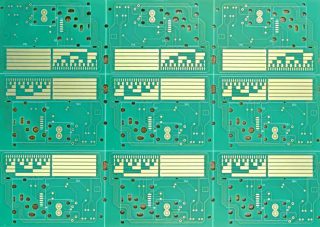
FR4 is the most widely used material for Printed Circuit Boards (PCBs) because of its excellent balance of mechanical strength, electrical insulation, thermal performance, and cost-effectiveness.
One important electrical property of FR4 is its breakdown voltage, which describes the point at which the insulating material can no longer withstand the applied electrical stress.
Understanding FR4 breakdown voltage is particularly important when designing high-voltage PCBs, power electronics, industrial control systems, power supplies, EV electronics, and other applications requiring reliable electrical isolation.
However, FR4 breakdown voltage should not be considered alone. In practical PCB design, dielectric strength, dielectric thickness, creepage distance, clearance distance, humidity, contamination, temperature, and manufacturing quality all influence the actual insulation performance of a PCB.

FR4 Breakdown Voltage tester
Breakdown voltage is the voltage at which an insulating material loses its ability to resist electrical conduction and dielectric breakdown occurs.
For FR4, breakdown can occur through the dielectric material when the electric field exceeds the material’s dielectric strength.
This is different from electrical arcing across the PCB surface or through air.
Therefore, three concepts should be distinguished in high-voltage PCB design:
A PCB may use FR4 with excellent dielectric strength but still fail if the clearance or creepage distance is insufficient.
Several factors influence the dielectric performance of FR4.
Not all FR4 materials have identical electrical properties.
Different FR4 PCB materials may use different resin systems, glass styles, filler systems, and curing processes.
Therefore, the dielectric strength specified in the actual laminate datasheet should always be used for critical high-voltage designs.
Increasing the insulation thickness generally increases the voltage required to produce breakdown through the dielectric.
However, breakdown voltage should not simply be calculated by multiplying a typical dielectric-strength value by the total PCB thickness.
For multilayer PCBs, the relevant insulation distance may be the dielectric thickness between two copper layers, rather than the overall finished PCB thickness.
FR4 can absorb a small amount of moisture from the environment.
Moisture can reduce insulation resistance and negatively affect dielectric performance, especially under high humidity or contaminated operating conditions.
This is one reason environmental conditions should be considered when designing high-voltage PCB assemblies.
Elevated temperatures can affect the resin system and electrical properties of the laminate.
For applications operating continuously at elevated temperatures, designers should consider not only breakdown voltage but also Tg, thermal aging, material rating, and long-term reliability.
Voids, contamination, resin defects, poor lamination, conductive residues, and other manufacturing defects can reduce insulation reliability.
For multilayer high-voltage PCBs, lamination quality and dielectric consistency are especially important.
FR4 is generally considered a good electrical insulating material, but there is no single universal breakdown-voltage value for every FR4 laminate.
Typical published dielectric-strength values for FR4 materials can vary considerably depending on:
Some FR4 laminate datasheets may report dielectric strength in the range of approximately 20–50 kV/mm under specified laboratory test conditions, but this should be treated as a material property rather than a PCB operating-voltage rating.
A common mistake is to assume:
FR4 dielectric strength × PCB thickness = safe PCB operating voltage
For example, if a laminate datasheet specifies a dielectric strength of 40 kV/mm, this does not mean that a standard 1.6 mm PCB should be designed to operate continuously at 64 kV.
Actual PCB voltage capability is usually limited by other factors long before the theoretical bulk dielectric breakdown of the FR4 is reached.
These factors include:
For high-voltage designs, always use the laminate manufacturer’s datasheet together with the applicable electrical safety standard.
Although the terms are related, they are not exactly the same.
Dielectric strength is normally expressed as voltage per unit thickness, such as kV/mm.
Breakdown voltage refers to the actual voltage at which a particular insulation structure fails under specified test conditions.
For example, two PCB constructions made from the same FR4 material may have different breakdown voltages because their dielectric thicknesses, copper geometries, environmental conditions, and manufacturing structures are different.
This distinction is especially important for multilayer PCBs.
A 1.6 mm PCB may contain only a relatively thin dielectric layer between two adjacent copper planes. In that situation, the overall 1.6 mm finished board thickness is not the relevant insulation thickness.
Clearance is the shortest distance through air between two conductive parts.
For high-voltage circuits, insufficient clearance may cause arcing even when the FR4 material itself remains electrically intact.
Clearance requirements depend on factors including:
Creepage is the shortest path along the surface of an insulating material between two conductive parts.
Surface contamination, humidity, and the material’s Comparative Tracking Index (CTI) can influence creepage requirements.
For this reason, creepage and FR4 breakdown voltage should not be treated as the same design parameter.
For multilayer PCBs carrying high voltage between internal copper layers, dielectric thickness and laminate construction become particularly important.
The PCB stack-up should be reviewed carefully to ensure adequate insulation between high-voltage copper features.
This may require:
Electric-field concentration can occur around sharp copper features and narrow gaps.
Smooth copper geometry and adequate spacing can help reduce localized electrical stress.
In some high-voltage PCB designs, routed slots are introduced between high-voltage conductors to increase the effective creepage path.
This can be particularly useful where PCB space is limited, although the design must still comply with the applicable safety requirements.
When designing a high-voltage PCB, FR4 breakdown voltage should be considered as part of the complete insulation system.
For a high-voltage PCB Board, FR4 breakdown voltage should be considered as part of the complete insulation system rather than as an isolated material specification.
Important considerations include:
Maintain sufficient spacing between high-voltage conductors according to the operating voltage and applicable safety requirements.
Select an FR4 grade with suitable dielectric properties, CTI, Tg, thermal performance, and environmental reliability.
For multilayer PCBs, specify adequate dielectric thickness between high-voltage copper layers.
For harsh environments, conformal coating or other protection methods may help improve surface insulation reliability.
However, conformal coating does not change the inherent bulk dielectric strength of FR4.
High-voltage PCB reliability also depends on manufacturing quality.
Lamination voids, contamination, insufficient spacing after etching, drilling defects, and other process variations can influence electrical insulation performance.
FR4 dielectric performance is particularly important in applications such as:
In these applications, the PCB should be evaluated as a complete insulation structure rather than based solely on the nominal dielectric strength of FR4.
FR4 dielectric performance can be evaluated using standardized material and electrical testing methods.
Common references include ASTM D149 and IEC 60243 for dielectric-strength testing of insulating materials.
Voltage is applied across an insulating sample under controlled conditions until electrical breakdown occurs.
The result provides information about the dielectric strength of the material under those particular test conditions.
A High-Potential (Hi-Pot) test applies a specified high voltage between isolated conductive sections for a defined period.
Unlike destructive dielectric breakdown testing, Hi-Pot testing is normally used to verify that an assembled product or PCB insulation system can withstand a specified test voltage without excessive leakage or breakdown.
Insulation resistance testing measures resistance between electrically isolated conductors.
This can help identify contamination, moisture, leakage paths, and other insulation problems.
These tests evaluate the electrical resistance of the insulating material along its surface and through its volume.
This distinction is important in PCB engineering.
FR4 breakdown voltage represents the point where dielectric failure occurs under specified test conditions.
Hi-Pot voltage, however, is a defined test voltage used to verify insulation integrity.
A PCB does not need to be driven to dielectric breakdown during routine production testing.
For example, a customer may specify:
500 VDC / 60 seconds, no breakdown or flashover.
This is a Hi-Pot test requirement, not the breakdown-voltage rating of the FR4 material.
The exact test voltage and duration should always follow the product specification or applicable safety standard.
Material selection is only one part of high-voltage PCB reliability.
From a PCB manufacturing perspective, several process factors deserve particular attention:
For multilayer high-voltage PCBs, a small manufacturing defect inside the stack-up may become an electrical weak point.
This is why high-voltage PCB projects should be reviewed jointly from design, material, stack-up, manufacturing, and testing perspectives.
Working with an experienced PCB supplier is also important for high-voltage projects, because material selection, stack-up design, lamination quality, spacing control, and electrical testing can all affect final insulation reliability.
FR4 breakdown voltage is an important material property for high-voltage PCB design, but it should never be considered in isolation.
Reliable high-voltage PCB design requires engineers to consider:
The key principle is simple:
A high dielectric-strength material does not automatically guarantee a high-voltage PCB.
The complete PCB insulation system must be designed and manufactured correctly.
For high-voltage, industrial, and high-reliability PCB projects, SQPCB provides engineering review, PCB fabrication, stack-up support, and manufacturing process control to help customers reduce potential insulation and reliability risks.
There is no universal value for all FR4 materials. Published dielectric-strength values can vary significantly depending on the laminate grade, thickness, conditioning, test direction, and test method. Some materials may show values in the approximate range of 20–50 kV/mm under specified laboratory conditions.
Always refer to the actual laminate manufacturer’s datasheet for engineering calculations.
You should not calculate the safe operating voltage simply by multiplying FR4 dielectric strength by the total PCB thickness.
In a real PCB, clearance, creepage, copper geometry, humidity, contamination, internal dielectric thickness, and applicable safety requirements may become limiting factors long before bulk FR4 breakdown occurs.
Yes. Moisture can reduce insulation resistance and affect dielectric performance. High-humidity applications therefore require additional attention to material selection, creepage, cleanliness, and environmental protection.
Conformal coating does not change the inherent bulk dielectric strength of FR4.
However, it can improve surface insulation performance and protect the PCB against moisture, contamination, and environmental exposure when correctly selected and applied.
Not necessarily.
Greater dielectric thickness can improve insulation between conductors, but high-voltage PCB design also depends on clearance, creepage, CTI, stack-up, copper geometry, environmental conditions, and safety requirements.
FR4 breakdown voltage refers to dielectric failure of the insulating material under specified conditions.
Hi-Pot voltage is a defined test voltage used to verify that an insulation system can withstand a specified electrical stress without breakdown or excessive leakage.
Solder mask can provide additional surface insulation and environmental protection, but it should not normally be used as the primary insulation method unless the applicable design standard specifically allows it.
High-voltage PCB design should first provide adequate creepage, clearance, and base-material insulation.
For high-voltage PCB projects, it is helpful to specify the working voltage, maximum transient voltage, required clearance and creepage, material requirements, stack-up, CTI requirement if applicable, operating environment, and any required Hi-Pot test voltage and duration.