As technology advances, transparent PCB boards have emerged as an innovative and futuristic trend in the printed circuit board (PCB) industry. These boards offer a unique combination of aesthetic appeal, flexibility, and practical applications, making them increasingly popular across various industries.
But what exactly is a transparent PCB board, and how does it differ from traditional PCBs? This article explores the definition, features, manufacturing process, applications, and challenges of transparent PCBs while highlighting their growing impact on modern electronics.
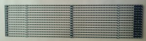
Transparent PCB Board
What is a Transparent PCBs?
A transparent PCB board is a circuit board with a clear or semi-transparent structure, allowing users to see through it while still maintaining full electrical functionality. Unlike traditional rigid PCBs, transparent PCBs are typically flexible circuit boards that use transparent PET film (polyethylene terephthalate) as the base material.
Key Characteristics:
✔ Made from transparent PET materials, which can be clear, pure white, light blue, or light green.
✔ Uses special transparent conductive materials, such as indium tin oxide (ITO) films or transparent conductive polymers, instead of standard copper conductors.
✔ Manufactured using processes similar to flexible printed circuit boards (FPCs), making them lightweight, flexible, and versatile.
✔ Provides high light transmittance and low reflectance, making them ideal for optical and display-based applications.
Features of Transparent PCB Boards
Transparent PCBs offer numerous advantages that set them apart from traditional PCBs. These features make them highly suitable for modern electronic applications.
1. High Flexibility & Mechanical Adaptability
🔹 Can be bent, folded, rolled, stretched, and moved freely in three-dimensional space.
🔹 Ideal for applications where flexible and dynamic circuit designs are required.
2. Superior Heat Dissipation & Compact Design
🔹 The transparent FPC (flexible PCB) structure allows for better thermal management, reducing overheating issues.
🔹 Enables miniaturization and lightweight product designs, making them ideal for wearables and ultra-thin devices.
3. Enhanced Aesthetic Appeal
🔹 Transparent PCBs enhance the visual appeal of devices, allowing manufacturers to showcase internal circuitry.
🔹 Ideal for luxury electronics, transparent displays, and gaming devices where aesthetics matter.
4. High-Performance Integration
🔹 Supports integrated components and compact wiring, improving device efficiency.
🔹 Ensures reliable electrical and mechanical performance despite its transparency.
5. Broad Compatibility with Electronic Devices
🔹 Transparent PCB boards are used in consumer electronics, medical devices, industrial automation, optical sensors, and communication equipment.
🔹 Compatible with both rigid and flexible PCB designs, offering adaptability to different industries.
Manufacturing Process
Key Steps in Production:
1️⃣ Material Selection – Using transparent PET film as the base material to maintain clarity.
2️⃣ Layer Formation – Applying transparent conductive materials like ITO or conductive polymers for electrical connectivity.
3️⃣ Etching and Patterning – Implementing fine-line etching to create circuits while preserving transparency.
4️⃣ Component Mounting – Utilizing low-temperature soldering methods to prevent damage to transparent materials.
5️⃣ Quality Inspection – Ensuring high optical clarity and electrical performance using Automated Optical Inspection (AOI) techniques.
Since transparent PCB materials are heat-sensitive, the entire production process requires precise temperature and environmental control to maintain both transparency and durability.
Applications
Transparent PCBs have found applications across various industries, revolutionizing how electronic circuits are used in aesthetic and functional designs.
1. Consumer Electronics
📱 Smartphones & Tablets – Transparent PCBs allow for see-through casing designs and futuristic edge-lit displays.
🎮 Gaming Devices – Enhances the visual appeal of gaming consoles and accessories with illuminated circuit visibility.
🏠 High-End Home Appliances – Integrated into luxury electronics for sleek, modern designs.
2. Wearable Technology
⌚ Smartwatches & Fitness Trackers – Transparent PCBs enable lighter, thinner, and more flexible designs.
👕 E-Textiles & Smart Clothing – Integrated into wearable tech for real-time health monitoring and IoT applications.
3. Medical Devices & Healthcare Technology
🏥 Diagnostic Equipment – Used in high-precision imaging devices like MRI and ultrasound machines.
💊 Implantable Medical Devices – Transparent PCBs allow for smaller, biocompatible medical circuits.
4. Industrial & Automation Systems
⚙ Instrumentation & Measurement Equipment – Improves sensor integration and automation control.
🚀 Robotics & AI Systems – Supports advanced vision-based and optical sensors for industrial robotics.
5. Optoelectronic & Display Technology
📺 Transparent Displays – Essential for see-through screens, AR/VR devices, and HUD systems.
🔬 Optical Sensors & Camera Modules – Improves light transmittance and performance in optical electronics.
Challenges in Designing
Despite their numerous advantages, transparent PCBs present unique technical challenges:
1. Material Limitations & Electrical Conductivity
⚠ Transparent PET and conductive polymers may have higher resistance than traditional copper.
⚠ Engineers must optimize circuit layouts to reduce signal loss and electrical inefficiencies.
2. Manufacturing Complexity & Cost
⚠ Requires specialized fabrication techniques to maintain transparency.
⚠ The cost of transparent materials is higher than standard FR-4 or ceramic PCBs.
3. Environmental Sensitivity
⚠ Transparent PCBs are more sensitive to humidity, temperature, and UV exposure, requiring extra protection.
⚠ Additional protective coatings may be needed to ensure long-term reliability.
To overcome these challenges, continuous innovation in materials, fabrication techniques, and protective coatings is necessary.
The Future
As the demand for innovative, lightweight, and aesthetically appealing electronics grows, transparent PCB technology is expected to evolve further.
Emerging Trends:
🔹 Flexible & Stretchable PCBs – Enabling wearable and bio-integrated devices.
🔹 AI-Driven PCB Design – Automating transparent circuit layouts for higher efficiency.
🔹 Sustainable Manufacturing – Reducing waste and environmental impact with eco-friendly materials.
🔹 5G & IoT Integration – Enhancing wireless connectivity in transparent electronics.
By continuously improving the design and manufacturing of transparent PCBs, engineers can unlock new applications and market opportunities in next-generation electronics.
Conclusion
Transparent PCB boards represent a revolutionary advancement in circuit board technology, offering flexibility, aesthetic appeal, and high-performance applications.
- They enhance device miniaturization, improve design aesthetics, and support emerging technologies like IoT and wearable electronics.
- Despite some manufacturing challenges, transparent PCBs are becoming a key trend in modern electronic innovation.
As research and development continue, transparent PCBs will become even more advanced, cost-effective, and widely adopted, shaping the future of electronic design.
our linkedin sqpcb.com

- long board pcb
- Flexible PCBs
- Special PCB
- Express Printed Circuit Board
- Pcb Prototype
- LED PCB
- PCB
- Printed Circuit Board
- Pcb meaning
- Pcb manufacturer
- Rigid pcb board
- Rigid Flex PCB
 Quote
Quote
 E-mail