What is a PCB Board? Definition, Components & Manufacturing Process
What Is a PCB Board:Imagine this: the sleek smartphone in your hand, the computer humming on your desk, or the high-tech medical device saving lives in hospitals—none of these would exist without a humble hero. Beneath their polished exteriors lies the beating heart of modern technology: the printed circuit board (PCB).
PCBs are the silent orchestrators of technology, transforming chaotic tangles of wires into sleek, efficient pathways for electrical currents. But what exactly are they? How do they work? And why are they indispensable in our everyday lives? Let’s dive into the fascinating world of PCBs to uncover their importance.
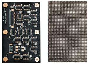
What Is a PCB Board?
A printed circuit board (PCB) is the foundational component of most electronic devices. It is a flat, rigid structure made from non-conductive materials like fiberglass or plastic, layered with conductive pathways. These pathways, often made of copper, act as highways for electrical signals, enabling components like resistors, capacitors, and microchips to work together seamlessly.
Key Features of a PCB
Efficient Design: Replaces bulky wiring with compact pathways.
Durability: Built to last with reliable materials.
Scalability: From single-layer designs to complex multi-layer boards.
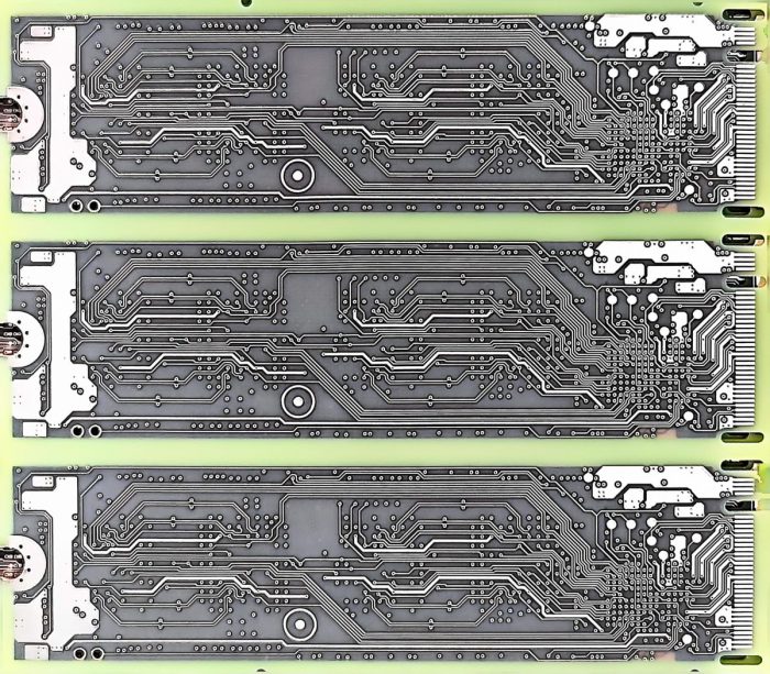
Why Are PCBs Essential?
PCBs revolutionized electronics by introducing compact and reliable designs. Before their invention, engineers relied on messy, error-prone point-to-point wiring. PCBs eliminated these issues and enabled the creation of smaller, faster, and more efficient devices.
Today, PCBs are found everywhere—in smartphones, laptops, medical devices, space shuttles, and more. Their versatility and reliability make them the backbone of modern technology.
Types of PCB Boards
Understanding the different types of PCBs helps in selecting the right one for specific applications:
Single-Layer PCBs: The simplest and most cost-effective design, ideal for basic devices like calculators and remote controls.
Double-Layer PCBs: Features conductive layers on both sides, used in applications like LED lighting and printers.
Multi-Layer PCBs: Stacks multiple layers of circuitry, enabling high-performance devices like smartphones and advanced medical equipment.
Flexible PCBs: Made from bendable materials, commonly found in wearable electronics and medical implants.
Rigid PCBs: Durable and sturdy, suitable for industrial machinery and automotive electronics.
Aluminum PCBs: Known for excellent heat dissipation, ideal for high-power applications like LED lights and power converters.
How Are PCBs Made? PCB Board Manufacturing Process
1. PCB Boards Manufacturing: Cutting the Raw Material
The manufacturing process begins with cutting the raw PCB material. The material, typically fiberglass-reinforced copper foil, is cut to the required size. The accuracy of cutting is critical, with a tolerance of +/-2mm. Common material sheet sizes include 36”*48”, 40”*48”, and 42”*48”. Material utilization is important for reducing waste, and in special cases, materials can be mixed for cutting to optimize production efficiency.

2. PCB Boards Manufacturing: Inner Layer Processing
This stage involves several sub-processes:
Pre-treatment: Cleaning and preparing the laminate to ensure a contaminant-free surface.
Coating: Applying a photosensitive coating on the laminate surface.
Exposure: Using a photomask to expose the coating to UV light, transferring the design pattern onto the laminate.
Development and Etching: Developing the exposed pattern and removing unwanted copper using a chemical etching solution.
Drilling: Drilling holes for vias and component leads.
AOI (Automated Optical Inspection): Conducting visual inspection to ensure quality.
At SQPCB, advanced techniques such as LDI (Laser Direct Imaging) exposure machines and fully automated coating and baking lines are used. The use of LDI technology minimizes film shrinkage issues, ensuring precise alignment and reducing registration errors. This innovation helps maintain controlled shrinkage within 0.1um, improving the overall quality of the inner layers.
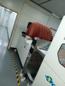
3. Lamination and Pressing
The lamination process involves the bonding of multiple layers to create multi-layer PCBs. This step includes:
Brown-Out and Riveting: Pre-pressing the laminate to form a stable base.
Pre-Stacking: Aligning the stacked layers of copper, laminate, and prepregs.
Pressing: Applying heat and pressure to bond the layers together.
X-ray Drilling Targets: Drilling targets are aligned and inspected using X-ray systems.
Edge Trimming and Grinding: Trimming the edges and ensuring uniformity in thickness.
Pressing is one of the most critical steps in multi-layer PCB production. SQPCB has optimized this process by selecting structures that not only meet the required board thickness but also improve impedance control. Materials such as 7628 are selected over more expensive options like 2116, significantly reducing costs while ensuring high performance.
4. Drilling Process
Drilling is a crucial step for creating holes for vias and through-hole components. It involves:
Pre-Drilling: Initial drilling to prepare the material for deeper cuts.
Drill Bit Grinding: Ensuring the drill bits are sharpened to maintain precision.
Pinning and Drilling: Ensuring accurate hole placement and depth.
Drill Bit Retirement and Peak Polishing: Polishing drill bits after 3,000-5,000 holes to maintain their effectiveness.
SQPCB uses linear motor-driven drilling machines, ensuring high-speed and high-precision drilling. These machines guarantee hole accuracy and consistency, ensuring that all holes meet IPC standards with a tolerance of +/-2mil.
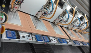
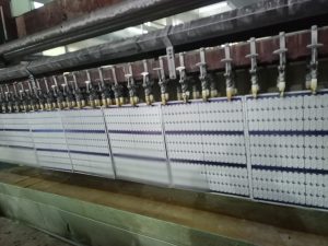
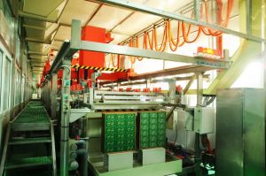
5. Electroplating Process
Electroplating is essential for copper deposition inside drilled holes and on the PCB surface. The process includes:
High-pressure Water Washing: Ensuring the board is clean before electroplating.
PTH (Plated Through-Hole): Plating copper inside the holes for electrical conductivity.
Copper Electroplating: Depositing a thin layer of copper onto the surface and inside the holes to ensure good electrical connections.
SQPCB uses renowned electroplating equipment, investing in high-quality systems that improve yield and reduce the failure rate. While equipment costs may be higher, the long-term benefits of reduced downtime and superior quality outweigh the initial investment.
6. Outer Layer Processing
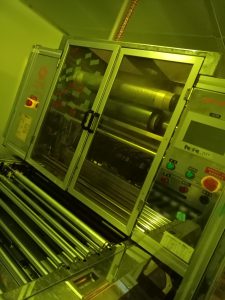
After the inner layers are completed, the outer layer processing begins. It includes:
Pre-treatment: Cleaning the copper surface before applying the protective coatings.
Film Lamination: Applying a protective film for further processing.
Exposure and Development: Using LDI technology to transfer the design onto the outer layer.
Etching and Removal: Removing the unwanted copper, leaving behind the designed circuit pattern.
AOI and Impedance Testing: Ensuring the design meets the required impedance and quality standards.
At SQPCB, LDI exposure machines with linear motor and optical scale control help achieve shrinkage accuracy within 0.1um, ensuring excellent alignment and reducing defects caused by manual handling.
7. Solder Mask Application
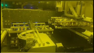
A solder mask is applied to the PCB to protect copper traces and prevent solder bridges during the assembly process. The steps include:
Pre-treatment and Silk Printing: Printing the solder mask onto the PCB.
Pre-baking: Pre-curing the solder mask to harden it before exposure.
Exposure and Development: Using UV light to expose and harden the mask where needed.
SQPCB implements automated solder mask applications, significantly reducing manual errors such as solder mask shift or incorrect pad coverage. This system helps maintain uniformity and ensures a high-quality finish for all PCBs.
8. Text and Legend Printing
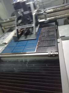
Text and legends are applied to the PCB to mark components, references, and other essential information. The process includes:
Silk Screen and Inkjet Printing: Printing labels and other markings.
Post-Baking: Curing the printed ink to ensure durability.
SQPCB uses linear motor-driven inkjet printing machines, achieving exceptional control over shrinkage and print accuracy. This technology reduces defects caused by misalignment and guarantees clear, legible text.
9. Surface Finishing
A surface finish is applied to exposed copper areas to protect against oxidation and improve solderability. This step includes:
Gold Immersion (ENIG), HASL, or OSP: The choice of surface finish is based on customer requirements for durability and solderability.
10. Final Inspection and Electrical Testing
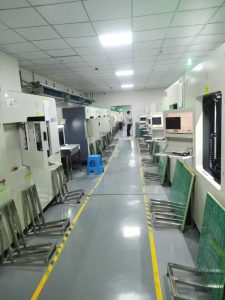
Before assembly, PCBs undergo a series of tests to ensure their functionality:
Electrical Testing: Detects open circuits, short circuits, or misalignments.
Flying Probe Testing and AOI: Ensure the PCB meets design specifications.
Final inspection is essential to ensure that no defects are present and the PCBs meet industry standards before packaging.
Advantages of PCBs
1. Compact Size:
Modern PCBs are designed to integrate a high density of components into a compact form, allowing for sleek, lightweight, and portable designs. This is particularly critical for advanced technologies such as smartphones, tablets, and wearable devices where space optimization is a priority.
2. High Reliability:PCBs offer a secure and stable platform for electrical components. The fixed connections and soldered joints significantly reduce the risk of loose connections, ensuring consistent and reliable performance even in high-stress or vibrating environments, such as automotive and aerospace applications.
3. Easy Maintenance:The organized layout of PCBs simplifies identification and troubleshooting of issues. Clear labeling and standardized design help technicians quickly locate faulty components, making repairs or replacements straightforward. This leads to reduced downtime and cost savings.
4. Enhanced Durability:With protective coatings such as solder masks, PCBs are resistant to environmental factors like moisture, dust, and corrosion. This ensures the longevity and consistent functionality of devices, even in harsh conditions.
5. Cost-Effective Mass Production:Once designed, PCBs are relatively inexpensive to mass-produce, thanks to automated manufacturing processes. This makes them a highly cost-efficient choice for industries producing large volumes of electronic devices.
6. Versatile Applications:PCBs are suitable for a wide range of applications, from simple consumer electronics to complex industrial, medical, and military equipment. They can be customized to fit the exact requirements of different industries, including multi-layered designs for sophisticated circuits.
7. Signal Integrity:PCBs are designed with precise paths for electrical signals, reducing electromagnetic interference (EMI) and ensuring minimal signal loss. This is crucial in high-frequency applications like telecommunications and data transfer systems.
8. Lightweight and Energy Efficient:Compared to traditional wiring methods, PCBs reduce the overall weight of a device. The conductive pathways on a PCB also minimize energy loss, making devices more energy-efficient.
9. Scalable Design Options:From single-layer to multi-layer and rigid to flexible designs, PCBs can be scaled to meet the specific needs of diverse applications, offering flexibility to designers and engineers in various fields.Would you like me to further elaborate or customize this content for a specific audience?
Challenges and Limitations
While PCBs are essential, they face challenges:
Thermal Management: Advanced designs require innovative cooling solutions.
Signal Interference: High-density circuits may encounter issues.
Cost: Custom or multi-layer PCBs can be expensive to produce.
How to Choose the Right PCB
Understand Your Requirements: Assess the complexity, durability, and performance needs of your project.
Collaborate with Experts: Partner with skilled manufacturers for customized solutions.
Verify Certifications: Look for ISO9001 and UL certifications for guaranteed quality.
The Future of PCBs
The PCB industry is evolving rapidly, with trends like:
IoT Integration: Smarter, more connected devices.
Miniaturization: Compact designs for advanced applications.
Sustainability: Use of eco-friendly materials and processes.
Conclusion
PCBs are the backbone of modern electronics, enabling innovation across industries. By understanding their design, types, and PCB manufacturing process, you can appreciate their critical role in shaping the future. Whether you’re an engineer or a curious learner, exploring PCBs unlocks a deeper understanding of the technology that powers our world.
For expert PCB manufacturing, explore our services at SQPCB.
- long board pcb
- Flexible PCBs
- Special PCB
- Express Printed Circuit Board
- Pcb Prototype
- LED PCB
- PCB
- Printed Circuit Board
- Pcb meaning
- Pcb manufacturer
- Rigid pcb board
- Rigid Flex PCB

 Quote
Quote
 E-mail