Introduction to Tooling-Hole in PCB
Printed Circuit Boards (PCBs) are the foundation of modern electronic devices, and their manufacturing process involves multiple stages of precision machining, assembly, and testing. One critical aspect of PCB fabrication and assembly is the tooling-hole, which serves as a crucial alignment and positioning feature during manufacturing.
A tooling hole is a non-plated or plated hole strategically placed on a PCB to facilitate alignment, registration, and handling throughout the fabrication and assembly processes. These holes are especially important in high-volume production environments, ensuring consistency, accuracy, and efficiency during manufacturing.
In this article, we will explore the significance of tooling holes, their types, design considerations, placement strategies, and the latest trends in PCB manufacturing.
tooling hole
The Importance of Tooling Holes in PCB Fabrication
In the complex world of Printed Circuit Board (PCB) manufacturing, precision and accuracy are critical. Every step of the production process—from drilling and etching to soldering and assembly—requires careful alignment to ensure that the final product functions correctly. One of the fundamental elements that enable this level of precision is the tooling hole.
A tooling hole is a specially designed hole placed on a PCB to facilitate alignment and positioning during manufacturing. These holes are used by drilling machines, soldering stations, and pick-and-place equipment to ensure that the PCB remains properly oriented throughout the production process. By providing fixed reference points, tooling holes help prevent misalignment, reduce production errors, and ensure consistency across multiple boards in large-scale manufacturing.
Without tooling holes, automated production lines would struggle to maintain accuracy, leading to higher defect rates, lower efficiency, and increased production costs. As the demand for high-density, multi-layered, and miniaturized PCBs continues to rise, tooling holes are becoming even more essential for maintaining precision in advanced PCB manufacturing.
Tooling Holes in PCB Design: A Key Feature for Manufacturers
The incorporation of tooling holes into PCB designs is a crucial step in ensuring that a board is manufacturable and compatible with industry-standard production techniques. Unlike vias or plated through-holes (PTHs), which are primarily used for electrical connections, tooling holes serve a mechanical purpose, guiding the PCB through each stage of its production lifecycle.
Manufacturers must carefully consider the size, shape, and placement of tooling holes to ensure that they are compatible with automated drilling, component placement, and soldering systems. In high-precision electronics, where even minor misalignments can result in device failures, the importance of correctly designed tooling holes cannot be overstated.
Additionally, panelized PCBs, where multiple smaller circuit boards are manufactured together on a single panel, rely heavily on tooling holes to ensure that each individual board is perfectly aligned before being separated. Without proper tooling hole placement, panel misalignment can lead to increased scrap rates and rework costs, reducing overall efficiency in mass production.
How Tooling Holes Improve Production Efficiency and Quality Control
One of the key advantages of tooling holes is their ability to enhance manufacturing efficiency while simultaneously improving quality control. By providing a consistent reference point for manufacturing equipment, tooling holes help to:
-
Ensure Proper Registration – During PCB drilling, etching, and solder mask application, the board must remain correctly aligned with production machines. Tooling holes serve as registration marks, ensuring that each layer of the PCB aligns correctly with the others.
-
Facilitate Automated Assembly – Modern PCB assembly lines rely heavily on pick-and-place machines, reflow soldering equipment, and optical inspection systems. Tooling holes allow these machines to accurately position and handle the PCB throughout the entire assembly process.
-
Reduce Manufacturing Errors – Misalignment in PCB production can cause short circuits, poor soldering connections, and defects that lead to costly failures. By using tooling holes, manufacturers can minimize these errors and improve overall yield rates.
-
Speed Up Inspection and Testing – Many automated optical inspection (AOI) and in-circuit testing (ICT) systems rely on tooling holes to correctly orient the PCB during testing. This ensures that defects such as misplaced components, soldering defects, and alignment issues can be quickly identified and corrected.
By integrating tooling holes into PCB designs from the very beginning, manufacturers can achieve higher production efficiency, better quality control, and improved product reliability.
Different Applications of Tooling Holes in PCB Manufacturing
The use of tooling holes is not limited to just fabrication and assembly—these features play a critical role throughout the entire PCB lifecycle, from initial prototyping to final testing and packaging. Some of the key applications of tooling holes in PCB manufacturing include:
1. PCB Fabrication and Layer Alignment
In multi-layer PCB manufacturing, multiple layers of copper and substrate material must be precisely aligned before they are laminated together. Tooling holes ensure that these layers are stacked correctly, preventing alignment errors that could affect circuit connectivity and signal integrity.
2. Automated Component Placement
During Surface Mount Technology (SMT) assembly, automated machines place tiny electronic components onto the PCB. Tooling holes help align the PCB on the placement machine’s conveyor, ensuring that each component is placed accurately according to the circuit design.
3. Soldering and Reflow Processing
In wave soldering and reflow soldering, the PCB must move through a heating process that melts solder and forms electrical connections. Tooling holes help keep the PCB in the correct position, preventing warping, shifting, or misalignment during soldering.
4. In-Circuit and Functional Testing
Before a PCB is integrated into a final product, it must undergo rigorous testing to ensure it meets quality standards. ICT and functional test fixtures use tooling holes to accurately position the board for electrical testing, ensuring that all circuits and components function correctly.
5. Depanelization and Final Assembly
Many PCBs are produced in panelized formats—multiple boards manufactured together and later separated. Tooling holes play a key role in ensuring that each PCB is properly aligned before depanelization, reducing mechanical stress and preventing board damage during final assembly.
By utilizing tooling holes across all stages of PCB production, manufacturers can achieve higher yields, improved product consistency, and reduced defect rates, making tooling holes an essential design consideration in modern electronics manufacturing.
Best Practices for Tooling-Hole Placement in PCB Design
When incorporating tooling holes into a PCB design, manufacturers must follow best practices to ensure maximum efficiency and compatibility with manufacturing processes. Here are some essential guidelines for tooling hole placement:
-
Strategic Positioning – Tooling holes should be placed at symmetrical locations on the PCB to ensure balanced alignment with production equipment. A three-point or four-point placement is typically recommended.
-
Standardized Hole Sizes – To ensure compatibility with common manufacturing fixtures, tooling hole diameters should follow industry standards (e.g., 1.5mm, 2.5mm, or 3.2mm).
-
Clearance from Critical Components – Tooling holes should not interfere with high-density component placements, traces, or via locations to avoid electrical and mechanical conflicts.
-
Panelization Considerations – When designing panelized PCBs, tooling holes should be aligned consistently across the entire panel to facilitate automated handling and depanelization.
-
Material Considerations – In flex PCBs and rigid-flex designs, tooling holes should be reinforced to prevent tearing or deformation during manufacturing.
By following these best practices, PCB designers and manufacturers can optimize tooling hole placement to improve manufacturability, alignment accuracy, and production efficiency.
Conclusion of Introduction
The tooling-hole may seem like a minor detail in PCB design, but its role in ensuring manufacturing precision, alignment, and efficiency cannot be overstated. From fabrication and assembly to testing and quality control, tooling holes provide a reliable reference point that enables automation, improves consistency, and reduces manufacturing defects.
As PCB technology continues to advance, tooling hole design will evolve alongside it, adapting to new manufacturing challenges and supporting high-density interconnect (HDI) designs, flexible electronics, and miniaturized circuit boards.
In the following sections of this article, we will explore detailed tooling hole design guidelines, manufacturing techniques, quality control measures, and emerging trends in PCB production, highlighting the indispensable role of tooling holes in the electronics industry.
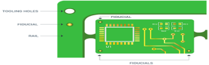
1. What is a Tooling-Hole in PCB?
A tooling-hole is a hole drilled into the PCB to help align the board with fixtures, machines, or manufacturing equipment during fabrication, assembly, and testing. These holes serve as reference points, allowing automated equipment to position the PCB correctly.
Why Are Tooling Holes Important?
-
Precise Alignment – Ensures accurate positioning of the PCB on fabrication machines, pick-and-place systems, and assembly fixtures.
-
Stable Handling – Helps secure the PCB in place, preventing movement during soldering, drilling, and routing.
-
Consistency – Reduces manufacturing variations, improving product uniformity in high-volume production.
-
Automation Compatibility – Supports automated assembly and inspection systems, enhancing production efficiency.
Tooling holes are widely used in various PCB types, including single-layer, double-layer, and multilayer PCBs, as well as in flexible circuits and rigid-flex designs.
2. Types of Tooling Hole in PCB Manufacturing
There are different types of tooling holes, each serving a specific purpose in the manufacturing process. The selection depends on the production stage and the machinery used.
1. Standard Tooling Holes
-
Typically round holes with diameters ranging from 1.5mm to 3.2mm.
-
Used for basic alignment and mechanical positioning.
-
Found in most PCBs, including rigid and flex circuits.
2. Fiducial Tooling Holes
-
Integrated with fiducial markers for optical alignment.
-
Essential in automated optical inspection (AOI) and pick-and-place machines.
-
Helps in achieving high precision for fine-pitch components like BGAs and CSPs.
3. Slotted Tooling-Holes
-
Elongated slots instead of round holes.
-
Used for PCBs requiring slight movement adjustments before final placement.
-
Common in high-precision assemblies where positional tolerance is tight.
4. Non-Plated Tooling-Holes
-
Used for mechanical alignment only without electrical conductivity.
-
Prevents unintended electrical connections and shorts.
-
Often seen in fixture-based testing and panelized PCBs.
5. Plated Tooling-Holes
-
Have a copper layer inside the hole, making them electrically conductive.
-
Used when grounding or electrical connectivity is needed for alignment.
-
Helps in electrostatic discharge (ESD) protection in sensitive electronic applications.
3. Design Guidelines for Tooling-Hole in PCB
Proper design of tooling-holes is essential to ensure compatibility with manufacturing equipment and improve PCB reliability. Here are the key design considerations:
1. Hole Size and Tolerance
-
Standard sizes range from 1.5mm to 3.2mm in diameter.
-
Tolerance: ±0.1mm for high-precision applications.
-
Should be compatible with drilling and punching equipment.
2. Placement Strategy
-
Symmetrical positioning improves balance and alignment.
-
Typically placed at three or four corners of the PCB.
-
Must be outside the critical circuit areas to avoid interference.
3. Spacing Considerations
-
At least 5mm from the PCB edges to prevent stress fractures.
-
Adequate spacing from vias and copper traces to avoid electrical shorts.
-
Should not be too close to component mounting pads to prevent mechanical stress.
4. Panelization and Array Design
-
Tooling holes must align across multiple PCBs in a panelized format.
-
Standard V-cut or breakaway tabs should not interfere with hole integrity.
-
Should support automated depaneling and assembly processes.
4. Tooling-Hole and PCB Manufacturing Process
Tooling holes play a critical role in various PCB manufacturing stages, from drilling to final assembly.
1. Drilling Process
-
High-speed CNC drilling machines create precise tooling-holes.
-
Laser drilling may be used for micro-hole applications.
2. Etching and Plating
-
If plated tooling holes are required, copper plating is applied.
-
Non-plated holes remain free of conductive material.
3. Solder Mask and Surface Finish
-
Holes are kept clear of solder mask for accurate mechanical fitting.
-
Surface finishes (HASL, ENIG, OSP) should not affect hole functionality.
4. Assembly and Testing
-
Tooling holes are crucial for SMT pick-and-place accuracy.
-
Used in AOI, in-circuit testing (ICT), and functional testing.
5. Quality Control for Tooling-Hole in PCB
To ensure reliability, manufacturers must implement strict quality control measures for tooling hole fabrication.
Inspection Methods:
-
Automated Optical Inspection (AOI) – Checks for misalignment and hole diameter accuracy.
-
X-ray Inspection – Verifies hole depth and plating integrity.
-
Mechanical Fit Testing – Ensures compatibility with alignment pins and fixtures.
Common Defects and Solutions:
| Defect | Cause | Solution |
|---|---|---|
| Misaligned holes | Drilling misregistration | Improve CNC calibration |
| Rough hole walls | Incorrect drill speed | Optimize drilling parameters |
| Copper peeling (Plated holes) | Poor adhesion | Use high-quality plating processes |
| Incorrect hole size | Tool wear or design error | Regular tool maintenance and DFM checks |
6. Future Trends in Tooling Hole for PCB Manufacturing
With advancements in PCB technology, tooling hole design and application are evolving to meet new challenges.
1. High-Precision Laser Drilling
-
Enables micro-tooling holes for miniaturized electronics.
-
Reduces stress on PCB material, improving durability.
2. Smart Manufacturing Integration
-
AI-powered vision systems for real-time alignment verification.
-
Automated robotic assembly reducing manual errors in PCB handling.
3. Flexible and Wearable PCB Applications
-
Advanced tooling hole designs for bendable and stretchable circuits.
-
Special reinforcement techniques for durability under stress conditions.
4. Sustainable PCB Manufacturing
-
Eco-friendly drilling and plating techniques to minimize waste.
-
Recyclable materials for tooling fixtures and PCB panels.
Conclusion: The Significance of Tooling-Holes in PCB Manufacturing
The tooling hole is an essential yet often overlooked feature in Printed Circuit Board (PCB) design and manufacturing. While it does not contribute directly to the electrical functionality of a PCB, its mechanical role is crucial in ensuring precision, alignment, and manufacturability. Throughout the PCB production process—ranging from drilling, layer stacking, soldering, and component placement to testing and final assembly—tooling holes serve as reliable reference points that enable efficient and accurate fabrication.
The Critical Role of Tooling-Holes in PCB Fabrication
From the very first steps of PCB production, tooling holes play an indispensable role. Layer alignment in multi-layer PCBs is a key area where tooling holes prove their importance. In modern PCB manufacturing, particularly in high-density interconnect (HDI) boards and flexible PCBs, precision alignment is critical. Even the slightest misalignment can result in trace mismatches, signal integrity issues, and increased defect rates.
Moreover, panelization—where multiple PCBs are fabricated on a single panel to optimize production efficiency—relies heavily on tooling-holes. These holes ensure that individual boards are correctly positioned within the panel, preventing misalignment during drilling, routing, and depanelization. Without tooling holes, registration errors could lead to uneven board separation, scrap rates, and increased production costs.
Another major advantage of tooling-holes is their role in automated production processes. As PCBs become more complex, the reliance on automated drilling machines, pick-and-place systems, and reflow soldering equipment has grown significantly. These machines use tooling-holes to precisely position and align PCBs, ensuring accurate component placement and soldering.
Tooling-Holes and Their Impact on PCB Assembly
During PCB assembly, especially in Surface Mount Technology (SMT) and Through-Hole Technology (THT) processes, tooling-holes assist in keeping the PCB properly oriented throughout the assembly line. SMT assembly involves placing tiny electronic components onto a PCB using high-speed robotic pick-and-place machines. These machines require accurate reference points to ensure that components are positioned correctly. Any misalignment in this stage can lead to defective solder joints, misplaced components, or circuit failures.
Similarly, in wave soldering and reflow soldering, proper alignment is critical to achieving strong and reliable electrical connections. Tooling-holes help guide the PCB through the soldering process, ensuring that solder paste is applied accurately and that components remain correctly positioned.
Additionally, automated inspection systems, such as Automated Optical Inspection (AOI) and In-Circuit Testing (ICT), rely on tooling-holes to position the PCB during quality checks. These inspections help detect defective solder joints, missing components, and electrical faults, improving overall product quality and reducing the risk of failures in the field.
Reducing Manufacturing Errors and Enhancing Quality Control
One of the most significant benefits of incorporating tooling-holes in PCB design is the reduction of manufacturing defects and rework costs. Misalignment, poor component placement, and incorrect soldering can result in significant waste if PCBs fail quality checks. Tooling-holes help minimize these issues by ensuring consistent positioning throughout the production cycle.
Furthermore, tooling-holes facilitate repeatability in mass production. In large-scale PCB manufacturing, every board must be identical to maintain product consistency and reliability. Tooling-holes provide a standardized method for ensuring that each PCB aligns perfectly with the next, preventing variations that could lead to functional inconsistencies in electronic devices.
Another critical aspect of quality control is testing and debugging. Before a PCB is assembled into a final product, it must undergo rigorous functional and electrical testing. Many testing fixtures, such as bed-of-nails test systems, use tooling-holes to securely hold the PCB in place during testing. This prevents movement that could affect test accuracy, ensuring reliable and repeatable test results.
Challenges and Considerations in Tooling-Hole Design
Despite their many benefits, the design and placement of tooling-holes require careful consideration. Poorly positioned tooling-holes can lead to mechanical stress, board warpage, and even structural weaknesses in certain PCB layouts. Some of the key challenges associated with tooling-holes include:
-
Interference with Electrical Components – Tooling-holes should not interfere with critical circuit traces, vias, or sensitive components. Poor placement can cause signal integrity issues, electromagnetic interference (EMI), or even mechanical damage to adjacent components.
-
Size and Standardization – Tooling-hole diameters must align with industry standards to ensure compatibility with automated manufacturing equipment and assembly fixtures. Variations in hole size could result in improper board alignment or equipment incompatibility.
-
Placement on Flexible PCBs – In flex and rigid-flex PCB designs, tooling-hole placement must consider material flexibility to prevent tearing or deformation during handling and assembly.
-
Panelization and Depanelization – In panelized PCB designs, tooling-holes must be positioned consistently to ensure seamless separation during depanelization. Misaligned tooling-holes can lead to excessive mechanical stress, increasing the likelihood of board damage.
By addressing these design challenges, manufacturers can ensure that tooling-holes effectively contribute to a smoother, more reliable, and more efficient PCB production process.
The Future of Tooling-Holes in PCB Manufacturing
As PCB technology continues to evolve, so too will the role of tooling-holes in modern electronics manufacturing. With the rise of miniaturized, high-frequency, and high-speed circuit designs, the need for even greater precision in PCB fabrication is growing.
One of the key trends influencing tooling-hole usage is the advancement of high-density interconnect (HDI) PCBs. These PCBs feature fine-pitch components, microvias, and ultra-thin substrates, making precise alignment more critical than ever. Tooling hole technology will need to adapt to smaller-scale manufacturing tolerances and higher-resolution drilling techniques.
Additionally, the integration of Artificial Intelligence (AI) and Machine Learning (ML) in PCB design and manufacturing is improving the way tooling holes are utilized. AI-driven design software can optimize tooling hole placement for maximum efficiency and minimal interference, reducing manufacturing errors and increasing production yields.
Furthermore, environmental sustainability in PCB manufacturing is becoming a priority. As the industry moves toward eco-friendly materials and lead-free soldering, tooling hole placement strategies may need to accommodate new fabrication methods and materials while maintaining precision and efficiency.
Tooling-holes may not be the most glamorous or technologically advanced feature in PCB design, but their importance cannot be overstated. They are a foundational element that ensures accuracy, consistency, and efficiency in PCB production, contributing to lower defect rates, higher product reliability, and improved manufacturing throughput.
By incorporating well-designed tooling holes, manufacturers can achieve better alignment, reduced errors, and enhanced automation in PCB fabrication. As electronic devices become smaller, more powerful, and more complex, tooling holes will continue to play a vital role in ensuring that PCBs meet the highest standards of quality and performance.
With continuous advancements in manufacturing automation, AI-driven design tools, and high-precision PCB technologies, the future of tooling holes remains bright. By staying ahead of emerging trends and best practices, PCB manufacturers can leverage tooling-holes to streamline production, improve quality control, and maintain their competitive edge in the electronics industry.

- long board pcb
- Flexible PCBs
- Special PCB
- Express Printed Circuit Board
- Pcb Prototype
- LED PCB
- PCB
- Printed Circuit Board
- Pcb meaning
- Pcb manufacturer
- Rigid pcb board
- Rigid Flex PCB
 Quote
Quote
 E-mail