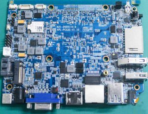
Printed Circuit Boards (PCBs) are the foundation of modern electronics, serving as the backbone for various electronic devices from smartphones to industrial machinery. The process of manufacturing and assembling a PCB is intricate and demands high precision to ensure the final product functions seamlessly. Here’s a step-by-step guide to understanding the key stages involved in PCB manufacturing assembly, focusing on achieving precision and maintaining high quality.

The PCB Manufacturing Assembly Process
1. Design and Layout
The PCB manufacturing process begins with designing the PCB layout. Engineers create the circuit design using specialized software (like Altium, Eagle, or KiCAD) that maps out the electronic connections between components. The layout includes traces, pads, and vias that establish the electrical connections on the board.
Once the design is finalized, it is checked for errors using a Design for Manufacturability (DFM) review. This ensures that the design meets the capabilities of the manufacturer and that potential issues are caught early.
2. Printing the PCB Design
After the design is verified, the next step is to print the PCB design onto the copper-clad board. This is done through a process known as photolithography, where a photoresist material is applied to the board. The design is then projected onto the board, hardening the photoresist in the areas corresponding to the circuit pattern.
Excess copper is etched away using chemical solutions, leaving only the copper traces that make up the PCB’s circuits.
3. Drilling Holes for Components
Once the copper pattern is established, the PCB is drilled to create holes for mounting components. The drilling process uses automated drilling machines that are capable of making holes as small as a few micrometers. These holes, also called vias, are used to connect different layers of the PCB and to insert through-hole components.
4. Layer Alignment and Lamination (for Multilayer PCBs)
For multilayer PCBs, individual layers are aligned and laminated together. Each layer consists of a substrate material, copper traces, and insulating material. Precise alignment is critical at this stage, as any misalignment can result in electrical faults.
The layers are pressed together under high temperature and pressure to form a solid PCB. After lamination, the board undergoes further inspection to ensure that all layers are aligned properly and that there are no defects.
5. Solder Mask Application
A solder mask is applied to the board to protect the copper traces and prevent short circuits during soldering. The solder mask is typically green, although other colors are available. This layer also improves the board’s durability and provides a surface for the solder to adhere to during component assembly.
6. Silkscreen Printing
The silkscreen layer is printed on the PCB to add labels, logos, and identifiers such as component values and part numbers. This layer helps in the assembly and testing process by providing reference information about the components and their placement on the board.
7. Component Placement
Once the PCB is fully prepared, the next stage is placing the components on the board. Modern PCB assembly processes typically use Surface Mount Technology (SMT), where components are placed directly onto the surface of the board. Automated pick-and-place machines precisely position each component based on the design.
For through-hole components, which require holes to be drilled in the PCB, the components are inserted by either automated or manual processes.
8. Soldering
After component placement, the PCB undergoes soldering, which securely attaches the components to the board. For SMT, reflow soldering is used, where the board is heated in a reflow oven to melt the solder and form solid connections. For through-hole components, wave soldering may be used, where the board passes over a wave of molten solder that attaches the components.
Both processes require precise temperature control to avoid damaging components and ensure reliable connections.
9. Inspection and Quality Control
Once soldering is complete, the assembled PCB undergoes rigorous inspection to detect any defects. Automated Optical Inspection (AOI) systems are commonly used to inspect solder joints and component placement. X-ray inspection is also used, particularly for boards with complex multilayer structures, to detect hidden defects like voids in solder joints.
Electrical testing, such as In-Circuit Testing (ICT) or Flying Probe Testing, is also performed to ensure that the PCB functions correctly and that there are no shorts, open circuits, or component failures.
10. Final Testing and Packaging
The final stage in the PCB manufacturing assembly process is functional testing, where the board is tested under real-world conditions to verify its performance. Any failed boards are either reworked or scrapped, depending on the severity of the defects.
Once the PCB passes all tests, it is cleaned, packaged, and shipped to the customer for integration into the final product.
Conclusion
The PCB manufacturing assembly process involves multiple stages, each critical to ensuring the precision and quality of the final product. From design and drilling to soldering and inspection, each step is vital in producing reliable, high-performance PCBs that power a wide range of modern electronics. As technological advancements continue, innovations in PCB manufacturing will further enhance efficiency, precision, and the ability to meet the evolving needs of various industries.
linkedin sqpcb.com
- long board pcb
- Flexible PCBs
- Special PCB
- Express Printed Circuit Board
- Pcb Prototype
- LED PCB
- PCB
- Printed Circuit Board
- Pcb meaning
- Pcb manufacturer
- Rigid pcb board
- Rigid Flex PCB

 Quote
Quote
 E-mail