Introduction to Stamp-Hole in PCB Manufacturing
In modern printed circuit board (PCB) manufacturing, the demand for precision, efficiency, and cost-effectiveness has led to the adoption of innovative techniques. One such method is the stamp hole process, which enhances the panelization and depanelization of PCBs. This method is particularly advantageous for high-volume production, cost-sensitive applications, and minimizing mechanical stress on PCB assemblies.
As electronic devices become smaller and more complex, the necessity of reliable and efficient board separation methods increases. The stamp-hole technique provides an optimal solution for these requirements, allowing for precise PCB breakout without excessive force or additional post-processing.
This article explores every aspect of stamp-hole usage in PCB fabrication, from its design considerations to manufacturing advantages, challenges, and future trends.
The stamp-hole method is widely utilized in high-volume PCB production, where manufacturers seek a balance between ease of separation, structural integrity, and manufacturing costs. It serves as an alternative to V-scoring and routing, particularly for irregularly shaped PCB designs. This technique is especially beneficial for consumer electronics, automotive PCBs, medical devices, and industrial control systems, where precise manufacturing and durability are essential.
As electronic devices continue to miniaturize, the demand for high-density and lightweight PCBs is increasing. The stamp hole approach provides a reliable and effective way to optimize PCB panel utilization while ensuring easy and controlled separation after the assembly process. This introduction will explore the fundamentals of stamp hole usage, its importance in PCB design and manufacturing, and the key factors to consider when implementing it.
stamp hole
stamp hole
1.1 Understanding the Role of Stamp-Hole in PCB Manufacturing
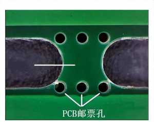
A stamp-hole is a series of small, partially drilled holes placed strategically along the edges of a PCB to create a breakaway point for easy separation. This method enables efficient depanelization, ensuring that the PCB remains intact without introducing excessive mechanical stress that could damage the board or its components.
Why Are Stamp-Holes Important?
-
Facilitates Efficient PCB Depanelization: Stamp-holes allow manufacturers to separate PCBs without additional cutting or complex machinery, streamlining production.
-
Reduces Mechanical Stress on the PCB: Compared to methods like V-scoring, which require high force during separation, stamp holes provide a more controlled and low-impact separation.
-
Cost-Effective Manufacturing Approach: The technique eliminates the need for additional cutting tools and reduces waste material, making it a cost-effective solution for large-scale production.
-
Supports Complex PCB Designs: Unlike V-scoring, which requires straight-line cuts, stamp-holes can be used on irregularly shaped PCBs, making them highly versatile for custom designs.
1.2 How Stamp-Hole Works in PCB Depanelization
The stamp-hole method is designed to create a weakened perforation line along the PCB, allowing for an easy and precise separation process. The key components of a stamp hole-based depanelization process include:
-
Hole Placement: Stamp-holes are strategically positioned along the PCB edge, ensuring they provide enough structural integrity during assembly while remaining easy to break when required.
-
Hole Size and Spacing: The holes are typically 0.5 mm to 1.0 mm in diameter, with a spacing of 0.8 mm to 1.5 mm to balance strength and breakability.
-
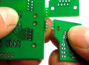
Separation Method: After assembly and testing, the PCB panel is gently snapped along the stamp hole line, cleanly separating individual boards without damaging components.
-
Post-Processing Considerations: In some cases, deburring or edge finishing may be needed to ensure the smoothness of separated edges.
By understanding how the stamp hole technique works, manufacturers can optimize their PCB designs to take advantage of this efficient and cost-saving method.
1.3 Considerations for Implementing Stamp-Holes in PCB Design
To effectively use stamp holes in PCB manufacturing, engineers must consider several key factors to ensure optimal performance:
1.3.1 Panel Strength and Stability
-
Stamp-holes should not weaken the PCB panel excessively, as this may cause damage during handling or assembly.
-
The spacing and number of holes should be carefully optimized to maintain the board’s structural integrity.
1.3.2 Component Placement Strategy
-
Avoid placing components too close to stamp holes, as the mechanical stress during separation may lead to damaged solder joints or component failures.
-
Sensitive components such as microcontrollers or BGA (ball grid array) chips should be positioned away from breakaway areas.
1.3.3 Post-Separation Quality Control
-
After PCB separation, manufacturers should inspect edges for roughness or burrs to ensure that boards meet quality standards.
-
In some cases, edge sanding or milling may be required to smooth the board’s edges.
1.4 Applications of Stamp Hole in Various Industries
The stamp hole method is widely used in different sectors where PCBs need to be panelized and efficiently depanelized:
1.4.1 Consumer Electronics
-
Commonly used in smartphones, tablets, and wearable devices to reduce manufacturing costs and increase production efficiency.
1.4.2 Automotive Industry
-
Applied in automotive control units, sensors, and infotainment systems, where high-reliability PCBs are required.
1.4.3 Medical Devices
-
Used in miniaturized PCBs for medical instruments, ensuring stress-free depanelization to protect delicate circuitry.
1.4.4 Industrial Equipment
-
Utilized in factory automation systems, power supplies, and control units where panelization optimizes mass production efficiency.
By implementing stamp hole techniques, these industries achieve high production efficiency, cost savings, and superior PCB quality.
1.5 The Growing Importance of Stamp-Hole in Future PCB Manufacturing
With continuous advancements in electronics and PCB manufacturing, the demand for efficient, low-stress depanelization methods is increasing. The stamp hole technique is expected to play an even greater role in next-generation PCBs, especially in the following areas:
-
Flexible and Rigid-Flex PCBs: As flexible electronics gain popularity, low-stress separation techniques like stamp holes will become more prevalent.
-
AI and Automated PCB Design: Future PCB designs will integrate AI-driven layout optimization, improving stamp hole placement for maximum efficiency.
-
Miniaturization of Electronic Components: As devices become smaller and more complex, stamp hole technology will evolve to meet new manufacturing challenges.
By staying at the forefront of innovation, manufacturers can leverage the stamp hole technique to create cost-effective, high-performance PCB solutions for the future of electronics.
2. What Is a Stamp-Hole in PCB Manufacturing?
A stamp-hole is a series of partially drilled holes placed in a specific pattern along the border of a PCB. These holes act as weak points, enabling easy separation of individual PCB units from a larger panel after assembly and testing. The stamp hole technique is an alternative to V-scoring and routing, offering a balance between mechanical strength and ease of separation.
How Stamp-Holes Function in PCB Design
-
Stamp holes are typically arranged in a row with small gaps between them.
-
The holes create a weakened breakaway area, allowing the board to be snapped apart when necessary.
-
This method reduces stress on PCB components compared to V-cut scoring, making it a preferred option for fragile or densely populated PCBs.
3. Advantages of Using Stamp-Hole in PCB Manufacturing
The stamp-hole method offers several advantages in PCB fabrication, especially for applications requiring panelized PCBs.
3.1 Cost-Effectiveness
-
Reduces the need for complex cutting tools, lowering manufacturing expenses.
-
Minimizes the use of additional depanelization machinery, making it ideal for mass production.
3.2 Less Mechanical Stress on Components
-
Unlike V-scoring or routing, stamp holes introduce less stress during PCB separation.
-
Beneficial for high-density PCBs with delicate surface-mounted components (SMDs).
3.3 Faster Depanelization Process
-
Enables quick and easy PCB separation without requiring specialized equipment.
-
Improves production efficiency, particularly in automated assembly lines.
3.4 Suitable for Odd-Shaped PCBs
-
Ideal for irregularly shaped boards, where V-scoring is difficult to apply.
-
Allows more flexibility in PCB design and layout optimization.
4. Key Design Considerations for Stamp-Hole in PCBs
To ensure the effectiveness and durability of stamp holes, careful design planning is essential.
4.1 Hole Size and Spacing
-
The diameter of stamp holes typically ranges between 0.5 mm to 1.0 mm.
-
Spacing between holes should be 0.8 mm to 1.5 mm to maintain mechanical stability while allowing easy separation.
4.2 Placement of Stamp-Holes
-
Should be positioned along the PCB panel edges, ensuring a uniform break line.
-
Avoid placing them too close to critical components, as mechanical stress during separation may cause damage.
4.3 Panelization Strategy
-
The number of stamp holes should be optimized to ensure structural integrity while still allowing smooth breakout.
-
Excessive stamp holes can lead to unwanted PCB flexing or incomplete separation.
5. Comparing Stamp-Hole with Other Depanelization Methods
Different PCB depanelization techniques are used based on cost, application, and mechanical requirements. The following comparison highlights the advantages and disadvantages of stamp-holes versus alternative methods.
5.1 Stamp Hole vs. V-Scoring
| Criteria | Stamp Hole | V-Scoring |
|---|---|---|
| Ease of Separation | Moderate | High |
| Mechanical Stress on PCB | Low | High |
| Suitability for Odd-Shaped PCBs | Excellent | Poor |
| Manufacturing Cost | Low | Medium |
| Ideal Application | Fragile PCBs | Rigid PCBs |
5.2 Stamp Hole vs. Routing
| Criteria | Stamp Hole | Routing |
|---|---|---|
| Material Waste | Minimal | High |
| Depanelization Speed | Fast | Slow |
| Precision | Moderate | High |
| Cost | Low | High |
| Tool Wear | None | High |
6. Challenges and Limitations of Stamp-Hole Usage
While stamp holes offer numerous benefits, they also come with certain challenges that PCB designers and manufacturers must address.
6.1 Structural Weakness
-
Excessive use of stamp holes reduces PCB panel strength, leading to warpage or breakage during handling.
-
Solution: Optimize hole spacing and panel reinforcement where needed.
6.2 Incomplete Separation Issues
-
Some PCBs may not cleanly break apart, leaving rough edges or excess burrs.
-
Solution: Use optimized hole placement and drilling precision.
6.3 Limited Suitability for High-Precision Boards
-
Stamp hole separation may not be suitable for ultra-high precision or microelectronics.
-
Solution: Use laser cutting or CNC routing for extreme precision applications.
7. The Future of Stamp-Hole in PCB Manufacturing
As PCB manufacturing technology advances, stamp hole techniques will continue to evolve to meet the demands of high-density interconnect (HDI) PCBs, flexible PCBs, and miniaturized circuits.
7.1 Emerging Innovations
-
Automated Stamp Hole Design Optimization using AI-driven CAD software.
-
Hybrid Depanelization Techniques, combining stamp holes with precision laser cutting.
-
Advanced PCB Materials that enhance panel stability while maintaining easy breakaway.
7.2 Expanding Industry Applications
-
Wearable Electronics: Miniaturized PCBs require low-stress separation methods.
-
Automotive PCBs: Increasing adoption in advanced driver assistance systems (ADAS) and EV power systems.
-
Medical Devices: Highly sensitive circuits demand stress-free separation for reliability.
Conclusion: The Role of Stamp-Hole in Next-Generation PCB Manufacturing
The stamp-hole technique has become an indispensable tool in modern PCB panelization, offering a cost-effective, low-stress, and efficient method for depanelization. As PCB designs continue to shrink while increasing in complexity, the need for precise and efficient depanelization methods will drive further innovations in stamp hole technology.
While alternative techniques like V-scoring and routing remain widely used, stamp holes provide unique advantages that make them the preferred choice for many PCB applications. As automated PCB assembly continues to evolve, the integration of AI-driven design tools and advanced laser-assisted depanelization will further enhance the precision and reliability of stamp hole-based PCB manufacturing.
By embracing optimized stamp hole designs, manufacturers can achieve higher yield rates, reduced production costs, and improved overall product quality, ensuring smoother PCB production for years to come.
As the electronics industry continues to evolve, PCB manufacturing must adapt to the increasing demand for efficiency, precision, and cost-effectiveness. The stamp hole method has proven to be a valuable depanelization technique that balances structural integrity, ease of separation, and cost-efficiency. As more industries integrate high-performance PCBs into their products, the stamp hole technique is expected to remain a critical aspect of modern PCB production.
This conclusion explores the impact, benefits, challenges, and future trends of using stamp holes in PCB manufacturing, helping designers and manufacturers make informed decisions about implementing this method in their production processes.
2.1 The Lasting Impact of Stamp-Hole in PCB Depanelization
2.1.1 Why Stamp Hole Continues to Be Relevant
Despite the introduction of advanced PCB depanelization methods, stamp holes continue to be widely used due to their simplicity and effectiveness. The main reasons behind their lasting impact include:
-
Efficiency in High-Volume Production: The ability to easily separate multiple PCBs from a panel using simple manual or automated methods makes stamp holes an ideal choice for mass production.
-
Reduced Mechanical Stress: Compared to other depanelization techniques such as V-scoring, stamp holes significantly reduce stress on PCB components, ensuring higher reliability.
-
Compatibility with Various PCB Designs: Unlike V-scoring, which requires straight lines, stamp holes can be placed along curved or irregular board edges, offering greater design flexibility.
-
Low-Cost Manufacturing: The simplicity of the stamp hole process minimizes production costs by eliminating the need for additional cutting tools or complex routing processes.
2.1.2 Industries That Benefit Most from Stamp-Hole Technology
Many industries benefit from using the stamp hole method in their PCB manufacturing, including:
-
Consumer Electronics: Smartphones, tablets, smartwatches, and other portable devices require cost-effective and reliable PCB depanelization methods.
-
Automotive Electronics: Sensor-based PCBs in modern vehicles rely on precisely manufactured circuit boards, where low-stress depanelization is essential.
-
Medical Devices: Delicate PCBs used in medical monitoring devices and diagnostic equipment benefit from stress-free depanelization, ensuring high reliability.
-
Industrial Automation: Control systems, power management circuits, and automation hardware depend on high-quality, precision-cut PCBs that the stamp hole method can provide.
The widespread application of stamp holes in these industries demonstrates their importance in modern PCB manufacturing.
2.2 Addressing Challenges in Stamp-Hole Implementation
Although stamp holes provide numerous advantages, manufacturers must address specific challenges to maximize efficiency and performance.
2.2.1 Optimizing Hole Placement and Density
-
Problem: Incorrect hole placement can lead to weak PCB panels or difficulty in separating boards.
-
Solution: Manufacturers should use simulation tools and industry best practices to determine optimal hole positioning.
2.2.2 Preventing Component Damage During Separation
-
Problem: Components placed too close to stamp holes may experience mechanical stress or solder joint damage.
-
Solution: Engineers should ensure that sensitive components are positioned away from depanelization areas.
2.2.3 Achieving Smooth Board Edges
-
Problem: The breaking process may leave rough edges or small burrs, which can affect assembly and product quality.
-
Solution: Post-separation processes such as sanding or edge finishing can improve the final product’s appearance and functionality.
By addressing these challenges, manufacturers can enhance the effectiveness of the stamp hole technique in PCB depanelization.
2.3 The Role of Automation and AI in Future Stamp-Hole Applications
2.3.1 How Automation is Improving Stamp-Hole Usage
With advancements in automation, PCB manufacturers are enhancing depanelization techniques using robotic systems and precision engineering. Automation helps in:
-
Ensuring Consistent Hole Placement: AI-driven PCB design tools can optimize the exact positioning and density of stamp-holes, improving manufacturing efficiency.
-
Reducing Errors and Waste: Automated depanelization machines minimize human error, ensuring clean and consistent board separation.
-
Increasing Production Speed: Robotics allow for fast and accurate board separation, reducing manufacturing cycle times.
2.3.2 AI-Driven Optimization for Future PCB Designs
AI is increasingly being used to optimize PCB layouts, including stamp-hole placement. AI-driven design tools:
-
Analyze stress distribution on the board to ensure optimal hole placement.
-
Optimize PCB panelization layouts to maximize material usage.
-
Predict potential structural weaknesses and adjust stamp hole positioning accordingly.
As AI continues to advance, the use of intelligent design systems will further enhance the effectiveness of stamp hole depanelization.
2.4 The Future of PCB Depanelization: Will Stamp-Holes Remain Relevant?
With the development of new depanelization techniques, manufacturers may question whether stamp-hole technology will continue to play a significant role in PCB production. However, several factors indicate that stamp holes will remain relevant in the coming years:
-
The Growing Demand for High-Volume Production
-
Stamp holes provide a fast and cost-effective method for depanelization, making them ideal for mass production.
-
-
Compatibility with Modern PCB Designs
-
As PCB shapes become more complex, stamp holes will remain useful for irregularly shaped boards.
-
-
Integration with Advanced Manufacturing Techniques
-
The combination of AI-driven PCB design and automation will further optimize stamp hole implementation, keeping it relevant in next-generation PCB production.
-
While laser cutting and CNC routing are becoming more common, the cost-effectiveness and simplicity of stamp hole depanelization ensure that it will continue to be a widely used method in PCB manufacturing.
2.5 Final Thoughts: Why Stamp-Hole is Essential for Modern PCB Manufacturing
Stamp-hole technology has been a proven and reliable depanelization method in PCB manufacturing for many years. Its efficiency, affordability, and compatibility with complex PCB designs make it an essential tool for manufacturers worldwide.
Key Takeaways from This Discussion:
-
Stamp holes provide an effective method for PCB depanelization, reducing mechanical stress and improving production efficiency.
-
Industries such as consumer electronics, automotive, and medical devices rely on stamp holes for precision PCB manufacturing.
-
Challenges such as optimal hole placement, post-separation quality, and component positioning must be addressed for successful implementation.
-
Automation and AI-driven design tools are revolutionizing stamp hole usage, optimizing panelization and improving manufacturing consistency.
-
Stamp holes will continue to be a valuable depanelization technique, even as newer methods like laser cutting gain popularity.
By continuing to refine and improve stamp hole technology, manufacturers can maximize efficiency and cost savings, ensuring that PCBs meet the high standards of reliability and performance required in today’s electronics industry.

- long board pcb
- Flexible PCBs
- Special PCB
- Express Printed Circuit Board
- Pcb Prototype
- LED PCB
- PCB
- Printed Circuit Board
- Pcb meaning
- Pcb manufacturer
- Rigid pcb board
- Rigid Flex PCB
 Quote
Quote
 E-mail