Introduction to Staggered Via Processes
Printed Circuit Board (PCB) technology has evolved significantly over the years to accommodate increasing miniaturization, higher signal integrity, and improved reliability. One of the essential innovations that have enabled these advancements is staggered via processes. These processes provide a more efficient and cost-effective approach to multilayer PCB design by improving connectivity between layers while maintaining the board’s mechanical and electrical integrity.
This article will provide an in-depth examination of staggered via processes, their role in PCB manufacturing, benefits, challenges, and future trends.
The rapid advancement of electronics technology has driven the demand for more compact, high-performance, and reliable printed circuit boards (PCBs). As devices shrink in size while increasing in complexity, manufacturers must optimize their PCB designs to accommodate high-speed signals, power distribution, and thermal efficiency. One crucial element of modern PCB fabrication is the integration of vias—electrically conductive pathways that link different layers of a circuit board.
Among various via technologies, staggered via processes have gained prominence due to their cost-effectiveness, mechanical strength, and signal integrity benefits. By employing a staggered rather than stacked arrangement, PCB designers can improve layer connectivity without excessive stress concentration, making these vias ideal for high-density interconnect (HDI) PCBs used in applications such as 5G technology, automotive electronics, industrial automation, and advanced medical devices.
This introduction provides a comprehensive overview of staggered via processes, their role in modern PCB manufacturing, and the factors influencing their adoption in today’s electronics industry.
Staggered via processes
1.1 Understanding Via Technology in PCB Design
Before delving into staggered via processes, it is essential to understand the role of vias in PCB interconnections. Vias are small holes drilled into a PCB and filled with conductive material to create electrical connections between different layers. They allow signals and power to travel between layers in multilayer PCBs, making them indispensable in complex circuit designs.
Types of PCB Vias
PCB vias can be classified into three primary categories:
-
Through-Hole Vias:
-
Extend through the entire PCB, connecting all layers.
-
Common in conventional and low-density designs.
-
Require mechanical drilling, increasing production costs.
-
-
Blind and Buried Vias:
-
Blind vias connect an external layer to an internal layer without passing through the entire PCB.
-
Buried vias connect internal layers without extending to outer surfaces.
-
Common in HDI PCBs, where space optimization is essential.
-
-
Microvias:
-
Small vias, usually less than 150 microns in diameter, created using laser drilling.
-
Used extensively in advanced HDI and flexible PCBs.
-
Vias can also be arranged in different structures, with the most common being stacked vias and staggered vias. The choice between these depends on manufacturing capabilities, cost constraints, and the performance requirements of the PCB.
1.2 The Evolution of Staggered Via Processes in HDI PCBs
The Shift Toward High-Density Interconnect (HDI) PCBs
With the proliferation of miniaturized consumer electronics, PCB designs have shifted toward high-density interconnect (HDI) technology. HDI PCBs allow for tighter trace routing, improved signal integrity, and better thermal performance.
One of the most significant design challenges in HDI PCBs is establishing layer-to-layer interconnections while preserving mechanical integrity and electrical performance. Traditional through-hole vias are impractical in HDI PCBs due to space limitations, leading to the adoption of microvias, blind vias, buried vias, and staggered via processes.
Transition from Stacked to Staggered Vias
Initially, stacked vias were the primary solution for multilayer interconnects in high-density PCB designs. However, stacked vias require precise alignment and additional processing steps, such as copper filling and electroplating, which increase fabrication complexity and cost.
The transition to staggered via processes was driven by the need to simplify manufacturing while maintaining electrical performance. Staggered vias are positioned in an offset manner, avoiding the direct alignment of via structures between adjacent layers. This reduces stress concentrations and delamination risks, improving the mechanical durability of HDI PCBs.
1.3 Key Benefits of Staggered Via Processes in PCB Manufacturing
1.3.1 Cost-Effectiveness and Manufacturing Simplicity
One of the major advantages of staggered vias is their lower production cost compared to stacked vias. The staggered arrangement eliminates the need for copper filling and additional plating steps, reducing the number of manufacturing cycles and material consumption.
1.3.2 Improved Mechanical Strength
Stacked vias create stress points where layers may delaminate or crack under thermal and mechanical stress. Staggered via processes distribute mechanical loads more evenly, enhancing the PCB’s structural reliability.
1.3.3 Enhanced Signal Integrity for High-Frequency Applications
In high-speed digital circuits and RF designs, signal integrity is critical. Staggered via processes minimize crosstalk and impedance mismatches by allowing better control over via placement and layer transitions. This makes them ideal for 5G networks, IoT devices, and aerospace applications.
1.3.4 Thermal Management Optimization
Staggered vias offer improved heat dissipation properties, reducing hotspots that could degrade PCB performance. This is especially important for power electronics and high-frequency designs, where effective thermal control is necessary to maintain reliability.
1.4 Challenges in Implementing Staggered Via Processes
1.4.1 Design Complexity and Simulation Requirements
Implementing staggered vias requires advanced PCB design software that supports precise via placement and signal integrity analysis. Engineers must simulate the electrical and thermal behavior of vias to optimize performance.
1.4.2 Manufacturing Precision and Alignment Issues
Since staggered vias are distributed across multiple layers, manufacturers must maintain tight tolerances in drilling, plating, and lamination processes to ensure proper electrical connectivity.
1.4.3 Compatibility with Advanced PCB Materials
While staggered vias work well with FR-4 and standard laminates, high-frequency substrates like Rogers or polyimide materials may require additional considerations for dielectric constant control and via reliability.
1.5 The Future of Staggered Via Processes in PCB Technology
1.5.1 AI and Machine Learning in Via Optimization
Emerging AI-driven PCB design tools are enhancing via placement strategies, allowing designers to automatically optimize staggered via arrangements for better electrical performance and manufacturability.
1.5.2 Advanced Laser Drilling Techniques
New ultra-precision laser drilling technologies are improving staggered via fabrication, allowing for smaller, more reliable microvias with better plating consistency.
1.5.3 Integration with 3D Packaging and Embedded Components
The future of staggered via processes will likely intersect with 3D IC packaging, where vias bridge PCB layers with embedded semiconductor components, creating highly integrated electronic solutions.
1.5.4 Sustainable and Lead-Free Manufacturing Processes
As environmental regulations become stricter, manufacturers are exploring eco-friendly materials and lead-free via plating technologies, ensuring that staggered via PCBs meet sustainability standards without compromising performance.
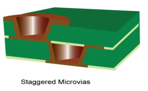
1.6 What Are Staggered Via Processes?
Staggered via processes refer to a PCB design technique in which microvias are positioned in a non-overlapping or staggered pattern across multiple layers. This method contrasts with stacked via processes, where vias are precisely aligned on top of each other.
Staggered vias are often employed in high-density interconnect (HDI) PCBs, where space constraints require optimal via placement without compromising electrical performance. These vias connect different layers of the PCB while reducing the risks associated with misalignment, stress concentration, and fabrication complexity.
1.6.1 Importance of Staggered Via Processes in Modern Electronics
With the rapid expansion of 5G technology, IoT devices, medical electronics, and high-performance computing, the need for densely packed PCBs has increased. Staggered via processes play a crucial role in enabling miniaturization while maintaining signal integrity.
Key advantages include:
-
Reduced stress on PCB layers, preventing delamination and cracks.
-
Lower fabrication costs compared to stacked vias.
-
Improved reliability in high-frequency and high-power applications.
-
Optimized thermal management, reducing hotspots and power dissipation issues.
1.6.2 Staggered Via vs. Stacked Via: A Comparison
| Feature | Staggered Via Processes | Stacked Via Processes |
|---|---|---|
| Alignment | Offset across layers | Directly stacked on top of each other |
| Fabrication Cost | Lower | Higher due to complex alignment |
| Reliability | Higher (less stress) | Moderate to high risk of failure |
| Electrical Performance | Excellent for high-speed signals | Good but requires precise plating |
| Mechanical Strength | More robust | Higher risk of delamination |
Given these advantages, staggered via processes are widely used in multilayer PCBs that require high-density interconnects with cost-efficient manufacturing.
2. The Role of Staggered Via Processes in PCB Fabrication
2.1 Layer Connectivity and Routing Optimization
Staggered via processes optimize PCB routing by reducing congestion in critical areas. By staggering vias across layers, designers can create more efficient signal pathways and minimize interference between layers. This is especially beneficial in RF circuits, high-speed digital applications, and power distribution networks.
2.2 Manufacturing Techniques for Staggered Vias
The fabrication of staggered vias involves sequential lamination processes, where layers are built up gradually, and vias are drilled using laser drilling or mechanical drilling techniques.
Key steps in staggered via fabrication:
-
Layer-by-layer construction: Each PCB layer is laminated sequentially, ensuring proper alignment.
-
Laser or mechanical drilling: Microvias are created using precision CO2 or UV laser drilling.
-
Electroplating and metallization: Copper is deposited inside the vias to ensure reliable electrical connections.
-
Inspection and testing: Advanced X-ray imaging and automated optical inspection (AOI) are used to detect defects.
2.3 Material Selection for Staggered Via Processes
The choice of materials significantly impacts the performance and reliability of staggered vias.
Key materials used in staggered via PCBs:
-
FR-4 (Flame Retardant-4): A cost-effective and widely used dielectric material.
-
High-frequency laminates (e.g., Rogers, Isola): Suitable for RF and microwave applications.
-
Polyimide-based substrates: Ideal for flexible and rigid-flex PCBs.
-
Copper foils with controlled thickness: Ensure consistent via plating and conductivity.
Material selection depends on application requirements, including signal speed, thermal performance, and mechanical durability.
3. Benefits and Challenges of Staggered Via Processes
3.1 Benefits of Staggered Via Processes
1. Cost-Effectiveness
Staggered vias reduce the complexity of fabrication, leading to lower production costs compared to stacked vias. Manufacturers can avoid expensive copper filling and electroplating techniques required for stacked vias.
2. Enhanced Reliability
By distributing mechanical stress across multiple layers, staggered via processes improve PCB lifespan and resistance to thermal cycling.
3. Better Signal Integrity
The non-overlapping nature of staggered vias minimizes crosstalk and signal degradation, making them ideal for high-frequency applications.
4. Improved Thermal Management
Staggered via designs allow for better heat dissipation, preventing localized heating issues in high-power applications.
3.2 Challenges and Limitations of Staggered Via Processes
Despite their advantages, staggered via processes come with certain challenges:
-
Complex design considerations: Requires advanced CAD software and simulation tools to optimize via placement.
-
Manufacturing precision: Requires highly accurate drilling and plating techniques to ensure via quality.
-
Limited vertical connectivity: While staggered vias provide horizontal routing advantages, they do not offer direct vertical interconnections like stacked vias.
4. Future Trends in Staggered Via Processes
The future of staggered via processes is driven by innovations in materials, fabrication techniques, and automation.
4.1 Advancements in Laser Drilling Technology
The development of high-precision laser drilling machines is enhancing the accuracy and consistency of staggered via creation.
4.2 AI-Powered PCB Design Automation
AI-based software tools are improving via placement optimization, leading to better electrical performance and cost efficiency.
4.3 Integration with 3D IC Packaging
As 3D semiconductor packaging evolves, staggered vias are being adapted to advanced interconnect solutions, bridging the gap between PCB and IC design.
4.4 Eco-Friendly PCB Manufacturing
Sustainable fabrication techniques, such as lead-free plating and recyclable laminates, are making staggered via processes environmentally friendly.
Conclusion: The Growing Importance of Staggered Via Processes
The adoption of staggered via processes is reshaping PCB manufacturing, providing a cost-effective, reliable, and high-performance alternative to traditional via structures. As industries demand smaller, more powerful electronic devices, the role of staggered vias in HDI PCB fabrication will continue to expand.
By addressing challenges in manufacturing precision and design complexity, staggered via processes will play a pivotal role in the future of high-speed, high-density PCBs. With ongoing advancements in laser drilling, AI-driven design automation, and eco-friendly materials, staggered vias will remain a cornerstone of next-generation electronic product development.
As the industry continues to evolve, staggered via processes will be integral to pushing the boundaries of PCB technology, enabling the next wave of innovation in consumer electronics, automotive systems, telecommunications, and beyond.
The continuous evolution of printed circuit board (PCB) technology is driven by the growing need for high-density, high-performance, and cost-effective solutions. Among the various interconnect methodologies, the staggered via process has proven to be a pivotal innovation, providing enhanced mechanical stability, electrical performance, and cost savings compared to alternative methods such as stacked vias. As PCBs become more complex to support 5G, IoT, artificial intelligence (AI), and high-speed computing applications, staggered vias are increasingly playing a critical role in ensuring efficient signal transmission, heat dissipation, and overall reliability.
This conclusion will revisit the significance of staggered via processes, explore their long-term benefits and future development, discuss potential challenges, and predict how the technology will continue to evolve to meet the needs of next-generation electronics.
3.1 Long-Term Benefits of Staggered Via Processes in PCB Manufacturing
3.1.1 Improved Structural Integrity and PCB Longevity
One of the most critical advantages of staggered vias is their ability to enhance the mechanical durability of PCBs. Unlike stacked vias, which require additional copper filling and careful alignment, staggered vias reduce localized stress concentrations, minimizing the risks of delamination, cracks, and via failure. As electronic devices become smaller and more powerful, ensuring long-term reliability is crucial, particularly for industries such as automotive, aerospace, and medical electronics, where failure can have severe consequences.
3.1.2 Optimized Electrical Performance for High-Frequency Applications
Modern electronics rely heavily on high-speed and high-frequency signals, requiring advanced PCB designs that can minimize signal integrity issues such as crosstalk, impedance mismatches, and electromagnetic interference (EMI). Staggered via processes help achieve consistent electrical performance by reducing the density of vertical interconnects, which in turn mitigates unwanted signal distortions. This makes them particularly advantageous in 5G base stations, radar systems, and ultra-high-speed computing platforms, where precise signal transmission is essential.
3.1.3 Manufacturing Efficiency and Cost Savings
The staggered via approach offers a simplified and cost-effective alternative to more complex via structures. By eliminating the need for precise laser-drilled microvias and expensive copper-filled vias, PCB manufacturers can reduce material costs and processing time while maintaining high-quality output. This makes staggered vias an ideal choice for mass production of consumer electronics, industrial automation systems, and telecommunications infrastructure.
3.2 Future Advancements in Staggered Via Technology
As PCB fabrication continues to advance, staggered via processes are expected to benefit from several key technological improvements, ensuring they remain a fundamental aspect of next-generation PCB design.
3.2.1 AI-Enhanced PCB Design and Simulation
Artificial intelligence (AI) and machine learning are revolutionizing PCB layout optimization by analyzing vast amounts of design data to recommend optimal via placements, signal routing strategies, and thermal management solutions. AI-driven PCB design tools will allow manufacturers to automate the staggered via design process, minimizing signal integrity issues and ensuring maximum efficiency in high-density PCB stack-ups.
3.2.2 Integration with Additive Manufacturing and 3D Printing
Additive manufacturing techniques, including 3D printing of PCBs, are becoming increasingly viable, allowing for the creation of complex via structures with unprecedented precision. By leveraging staggered vias within 3D-printed PCB designs, manufacturers will be able to fabricate highly compact, multi-layer boards with fewer manufacturing constraints and improved electrical performance.
3.2.3 Advancements in High-Frequency Materials
As RF and microwave applications demand higher signal integrity, PCB materials are evolving to include low-loss dielectrics, flexible substrates, and heat-resistant laminates. Staggered vias will need to be optimized for these next-generation materials, ensuring minimal signal distortion and enhanced durability in extreme environments.
3.3 Challenges in Scaling Staggered Via Processes for Mass Production
Despite their many benefits, scaling staggered via processes for large-scale PCB manufacturing presents several challenges that must be addressed.
3.3.1 Precision Control in High-Volume Manufacturing
Mass production of PCBs with staggered vias requires precise drilling, plating, and registration control to ensure that vias are aligned correctly within multi-layer stack-ups. Any misalignment could lead to short circuits, increased impedance, or mechanical failure, which necessitates strict quality control measures.
3.3.2 Compatibility with Emerging PCB Fabrication Techniques
As new PCB fabrication techniques—such as substrate-like PCBs (SLP), embedded component packaging, and flexible hybrid electronics (FHE)—gain traction, staggered via processes must be adapted to integrate seamlessly with these technologies. This may require innovative drilling and plating solutions, as well as redesigned CAD workflows that account for new material properties.
3.3.3 Trade-offs Between Cost and Performance
While staggered vias offer cost savings compared to stacked vias, they may not be the most cost-effective solution for every PCB design. Designers must carefully evaluate cost-benefit trade-offs based on signal integrity requirements, thermal constraints, and manufacturing feasibility to determine when staggered vias provide the greatest value.
3.4 The Growing Role of Staggered Via Processes in Next-Generation Electronics
The adoption of staggered via processes is expected to expand significantly in next-generation PCB applications, particularly in the following industries:
3.4.1 Telecommunications and 5G Infrastructure
With 5G and beyond requiring ultra-high-speed PCBs, staggered vias will play a crucial role in ensuring low-latency signal transmission, supporting the deployment of high-frequency antenna modules and data processing systems.
3.4.2 Automotive and Aerospace Electronics
Reliability is paramount in automotive and aerospace PCBs, where staggered vias will contribute to better mechanical strength, heat dissipation, and long-term durability in harsh environmental conditions.
3.4.3 Wearable and IoT Devices
Miniaturization remains a primary goal for wearable technology and IoT applications. Staggered via processes will enable compact, high-performance PCB layouts with improved flexibility and reliability.
3.4.4 Artificial Intelligence and High-Performance Computing
Next-generation AI processors, data centers, and high-performance computing (HPC) systems require efficient power distribution and high-speed signal routing. Staggered vias will help optimize these complex interconnect architectures, ensuring minimal signal degradation and thermal issues.
3.5 Final Thoughts: Why Staggered Via Processes Will Continue to Thrive
As electronic devices continue to evolve, the staggered via process will remain a cornerstone of PCB interconnect technology, offering a balance between mechanical strength, electrical performance, and manufacturing efficiency.
While challenges remain in scaling production, ensuring compatibility with new materials, and maintaining cost-effectiveness, ongoing advancements in AI-driven design tools, laser drilling precision, and next-generation manufacturing techniques will further enhance the capabilities of staggered via technology.
Ultimately, staggered via processes will continue to thrive as an integral component of future PCB designs, supporting industries ranging from consumer electronics to aerospace, 5G infrastructure, and AI-powered computing systems. As demand for higher performance and miniaturized devices grows, staggered via solutions will enable the next generation of cutting-edge electronic innovations.

- long board pcb
- Flexible PCBs
- Special PCB
- Express Printed Circuit Board
- Pcb Prototype
- LED PCB
- PCB
- Printed Circuit Board
- Pcb meaning
- Pcb manufacturer
- Rigid pcb board
- Rigid Flex PCB
 Quote
Quote
 E-mail