Introduction to Stacked Via Processes
Printed circuit boards (PCBs) have undergone significant advancements over the past few decades. As electronic devices continue to shrink while demanding greater performance, PCB interconnect strategies have had to evolve to accommodate these changes. Among the most significant developments in PCB design is the introduction of stacked via processes. This technique is particularly crucial for high-density interconnect (HDI) PCBs, where space constraints and high-speed signal integrity are key concerns.
Traditional PCB designs primarily relied on through-hole vias and buried vias, which worked well for conventional electronics. However, as the demand for compact and multi-functional devices increased, designers needed more efficient interconnection solutions. Stacked via processes emerged as a solution that allows multiple microvias to be stacked on top of one another across several PCB layers. This technique facilitates higher routing density, improved electrical performance, and better reliability in applications requiring complex multilayer PCBs.
With the rapid advancement of electronic devices, printed circuit boards (PCBs) have become more compact and complex. This miniaturization requires innovative interconnection techniques, one of which is stacked via processes. These processes allow electrical signals to pass through multiple layers of a PCB, ensuring optimal performance in high-density interconnect (HDI) designs.
In contrast to traditional through-hole vias, stacked vias enable direct vertical connections between multiple layers, reducing routing complexity and enhancing signal integrity. They are particularly useful in high-performance applications such as smartphones, automotive electronics, and industrial automation systems.
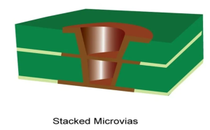
Stacked via processes
Understanding the Role of Vias in PCB Design
Vias are small holes in a PCB that create electrical connections between different layers. They serve as conduits that enable signals and power to travel efficiently across multiple layers of the board. The three main types of vias used in PCB design are:
-
Through-Hole Vias – These extend through the entire PCB and are primarily used in conventional multilayer designs.
-
Buried Vias – These are placed entirely within the internal layers of a PCB and do not extend to the outer layers.
-
Microvias – Small laser-drilled vias that connect adjacent layers, commonly used in HDI PCB designs.
Stacked via processes primarily involve microvias, which can be stacked in a vertical column to establish multi-layer connections. This stacking capability offers several advantages over traditional vias, particularly in complex, miniaturized electronic devices.
Why Stacked Via Processes Are Crucial for Modern PCBs
The rise of HDI PCB technology has driven the need for more advanced via structures. In modern electronic applications, designers are constantly seeking ways to reduce form factors while improving electrical performance. Stacked via processes meet these demands by enabling high-density interconnections without increasing the overall PCB size.
Key factors driving the adoption of stacked via processes include:
-
Miniaturization of electronic devices: Consumer electronics, such as smartphones, wearables, and IoT devices, require compact PCBs with increased routing density.
-
High-speed signal transmission: Many advanced applications, such as 5G networks, automotive electronics, and aerospace systems, require PCBs with minimal signal interference. Stacked vias help achieve shorter signal paths, improving overall system performance.
-
Power distribution efficiency: Stacked vias ensure better conductivity in power modules and high-performance computing boards, where stable power delivery is critical.
Stacked Vias vs. Other Via Configurations
Stacked vias are one of several via interconnection techniques used in modern PCB fabrication. However, it is essential to understand how they compare to other via configurations, such as staggered vias and buried vias, to determine their suitability for specific applications.
| Via Type | Description | Key Advantages | Key Disadvantages |
|---|---|---|---|
| Stacked Vias | Microvias stacked vertically to connect multiple layers. | High routing density, compact design, improved signal integrity. | Higher cost, complex manufacturing, potential reliability issues. |
| Staggered Vias | Microvias placed in a staggered formation across different layers. | Easier to manufacture, lower cost, improved reliability. | Requires more space than stacked vias, less efficient routing. |
| Buried Vias | Internal vias that do not extend to the outer layers. | Saves board space, improves electrical performance. | Increases fabrication complexity, requires precise alignment. |
| Through-Hole Vias | Extend through the entire PCB. | Strong mechanical reliability, easy to manufacture. | Consumes more board space, less effective in HDI PCBs. |
From the comparison above, stacked via processes offer superior advantages in miniaturized, high-performance PCB designs, making them the preferred choice for advanced applications.
The Role of Stacked Via Processes in HDI PCBs
High-density interconnect (HDI) PCBs have become a standard in smartphones, tablets, and advanced computing systems. These PCBs utilize multiple layers and require efficient routing techniques to maximize space utilization. Stacked via processes play a pivotal role in HDI PCBs by providing:
-
Compact and efficient signal routing, enabling complex circuits in smaller footprints.
-
Better power and ground plane connections, reducing impedance mismatches and improving overall stability.
-
Improved signal integrity and reduced electromagnetic interference (EMI) for high-speed data transmission.
By integrating stacked via processes into HDI PCBs, manufacturers can achieve greater component density and enhanced electrical performance while maintaining the mechanical integrity of the board.
Challenges in Stacked Via Fabrication
Despite their advantages, stacked via processes pose certain manufacturing challenges. The precise fabrication process requires highly advanced laser drilling, plating, and lamination techniques to ensure reliability. Some of the key challenges include:
-
Alignment Precision – Since stacked vias require multiple lamination and drilling steps, any misalignment can lead to connection failures.
-
Via Reliability – Poor plating or copper filling in stacked vias can result in electrical failures or mechanical weaknesses.
-
Manufacturing Cost – Due to the complexity of stacked via fabrication, costs are generally higher compared to traditional via processes.
To mitigate these challenges, advanced fabrication techniques, such as laser via drilling, controlled impedance design, and advanced electroplating, are employed to ensure consistent quality and performance.
Applications of Stacked Via Processes in Different Industries
Stacked via processes are widely used in various industries that demand high-performance and compact PCB designs. Some key application areas include:
-
Consumer Electronics – Smartphones, tablets, and laptops rely on stacked vias to reduce PCB size while maintaining high-speed performance.
-
Automotive Electronics – Advanced driver-assistance systems (ADAS) and electric vehicle (EV) power management systems benefit from stacked vias’ reliability and thermal efficiency.
-
Medical Devices – Miniaturized implantable and wearable medical electronics require highly dense PCBs, where stacked vias offer the best interconnection solution.
-
Aerospace and Defense – Military-grade and space-rated PCBs demand robust and compact designs, making stacked via processes an essential technology.
Future Trends in Stacked Via Technology
With continued advancements in electronics, stacked via processes are expected to evolve further to meet the increasing demands of smaller, faster, and more reliable PCBs. Some emerging trends in this field include:
-
Advancements in laser drilling technology to improve the precision of microvia fabrication.
-
New materials with better thermal and mechanical properties to enhance stacked via reliability.
-
Automated via inspection techniques, including AI-driven quality control, to detect defects during fabrication.
-
Integration of stacked vias with emerging semiconductor packaging techniques, such as 2.5D and 3D IC packaging, for even higher component density.
2. Types of Vias Used in Stacked Via Processes
2.1 Microvias
Microvias are small-diameter vias commonly used in HDI PCBs. These vias typically have a diameter of less than 150 µm and are created using laser drilling techniques.
2.2 Buried Vias
Buried vias connect internal layers of a PCB without reaching the outermost layers. These vias are typically formed during the board’s fabrication process and are useful in complex, multilayer designs.
2.3 Through-Hole Vias
Unlike microvias and buried vias, through-hole vias extend through the entire PCB thickness. While they provide strong mechanical support, they are less space-efficient in HDI applications.
3. Manufacturing Techniques for Stacked Via Processes
3.1 Sequential Lamination
Stacked via processes require multiple lamination steps, where layers are fabricated and then bonded together. Each layer contains drilled and plated vias, which are aligned to create stacked vias.
3.2 Laser Drilling
Since stacked vias require precise alignment, laser drilling is the preferred method for creating microvias. This technique ensures clean and accurately positioned holes.
3.3 Electroplating and Copper Filling
To ensure strong electrical connections, vias are filled with electroplated copper. This process eliminates voids and enhances the reliability of the stacked via structure.
4. Advantages of Stacked Via Processes
4.1 Space Efficiency
By stacking vias vertically, designers can create more compact and high-density PCBs, making them ideal for modern electronic devices.
4.2 Improved Electrical Performance
Stacked vias reduce the length of signal paths, minimizing impedance mismatches and enhancing overall electrical performance.
4.3 Better Thermal Management
Copper-filled stacked vias improve heat dissipation, reducing the risk of thermal damage in high-power applications.
5. Challenges and Limitations of Stacked Via Processes
5.1 Manufacturing Complexity
The precision required for stacked via processes increases manufacturing complexity, necessitating advanced equipment and expertise.
5.2 Cost Implications
Since stacked vias involve multiple fabrication steps, they can be more expensive compared to traditional via techniques.
5.3 Reliability Concerns
If not properly fabricated, stacked vias may suffer from issues like delamination, cracking, or plating voids, impacting the long-term reliability of the PCB.
6. Applications of Stacked Via Processes in PCBs
6.1 Consumer Electronics
Stacked vias enable the production of compact smartphones, tablets, and wearable devices.
6.2 Automotive and Aerospace Industries
High-performance PCBs with stacked vias are crucial for advanced driver-assistance systems (ADAS) and aerospace communication equipment.
6.3 High-Speed Communication Devices
Routers, servers, and 5G base stations benefit from the improved signal integrity provided by stacked vias.
7. Comparison: Stacked Via Processes vs. Staggered Via Processes
7.1 Key Differences
While stacked vias are aligned vertically, staggered vias are offset from each other, making them easier to manufacture but less space-efficient.
7.2 When to Choose Stacked Vias Over Staggered Vias
-
Choose stacked vias when space is limited and high signal integrity is required.
-
Use staggered vias when reducing manufacturing complexity and cost is a priority.
8. Future Trends in Stacked Via Processes
8.1 Innovations in Microvia Technology
Advancements in laser drilling and via plating techniques continue to improve the reliability and performance of stacked vias.
8.2 Material Advancements for Better Via Reliability
New dielectric materials with lower coefficients of thermal expansion (CTE) help prevent via failures due to thermal cycling.
9. Conclusion
Stacked via processes are a crucial innovation in PCB design, enabling the creation of high-density, high-performance electronic devices. Despite the challenges associated with manufacturing complexity and cost, their benefits in terms of space efficiency, electrical performance, and thermal management make them indispensable in modern electronics. As technology continues to evolve, advancements in microvia fabrication and material science will further enhance the reliability and efficiency of stacked vias, paving the way for more sophisticated PCB designs.
The advancement of stacked via processes has fundamentally transformed the way printed circuit boards (PCBs) are designed and manufactured. As the demand for smaller, faster, and more reliable electronic devices continues to rise, stacked vias have become an essential component in the high-density interconnect (HDI) PCB industry. These processes allow for enhanced routing efficiency, improved electrical performance, and superior mechanical stability, making them a key factor in modern PCB designs.
In this conclusion, we will explore the long-term impact of stacked via processes, discuss emerging trends and challenges, and highlight the potential advancements that will shape the future of PCB manufacturing.
The Increasing Role of Stacked Vias in Modern Electronics
As consumer electronics, automotive systems, medical devices, and aerospace technology continue to evolve, the need for high-performance PCBs is becoming more pressing. Stacked via processes have proven to be instrumental in achieving miniaturization without compromising performance, offering a viable solution for industries that require compact, high-speed, and reliable circuit boards.
1. High-Speed Data Transmission
In the digital age, high-speed signal integrity is critical for many applications, including 5G technology, high-performance computing, and advanced communication systems. Stacked via processes contribute to signal integrity by reducing transmission distances and minimizing electromagnetic interference (EMI). As PCBs continue to accommodate higher frequencies, stacked vias will play a central role in ensuring that electrical signals remain stable and efficient.
2. Miniaturization and Space Optimization
With the ongoing push toward miniaturization, especially in wearable technology and IoT devices, stacked via technology is becoming increasingly important. Traditional via structures often take up valuable board space, limiting design flexibility. Stacked vias, on the other hand, allow for multi-layer connections within a compact form factor, leading to higher routing density and better space utilization. This feature is particularly valuable in smartphones, tablets, and medical implants, where maximizing PCB real estate is a top priority.
3. Thermal Management and Power Distribution
Stacked via processes also contribute to better thermal management and power distribution, especially in high-power electronics such as electric vehicles (EVs) and industrial automation systems. Efficient power delivery and heat dissipation are essential to maintaining reliability and longevity in these applications. The strategic placement of stacked vias allows for optimized current flow and effective heat dissipation, reducing the risk of hotspots and electrical failures.
Challenges and Limitations in Stacked Via Processes
Despite their numerous advantages, stacked via processes come with their own set of challenges that need to be addressed to ensure long-term reliability and cost-effectiveness.
1. Complex Manufacturing and Higher Costs
One of the most significant challenges associated with stacked via processes is their complex manufacturing process. Compared to traditional via structures, stacked vias require precise alignment, advanced laser drilling, and multiple plating steps. These additional steps increase fabrication complexity, leading to higher production costs.
For many PCB manufacturers, achieving consistent via stacking quality is a major hurdle. Small misalignments or inconsistencies in copper plating thickness can lead to open circuits or reliability issues over time. To mitigate these risks, automated quality control measures, such as X-ray inspection and laser measurement systems, are being integrated into manufacturing processes.
2. Reliability and Mechanical Stability
Stacked vias are often subjected to mechanical stress, temperature fluctuations, and repeated thermal cycling during a PCB’s operational life. If not properly designed, these vias can become weak points in the circuit, leading to cracks, delamination, or electrical failures.
To improve long-term reliability, PCB manufacturers are investing in advanced via fill materials, better copper plating techniques, and reinforced lamination processes. Additionally, simulation software and finite element analysis (FEA) tools are being used to predict via performance under different operating conditions, ensuring that stacked vias remain stable even in extreme environments.
3. Integration with Advanced Packaging Technologies
The growing demand for heterogeneous integration and 3D packaging solutions has led to the convergence of PCB technology with semiconductor packaging techniques. As a result, stacked via processes must adapt to new interconnection methods, such as through-silicon vias (TSVs) and embedded die packaging.
To maintain compatibility with these emerging technologies, PCB manufacturers are developing new via stacking techniques, including semi-additive manufacturing (SAP) processes and ultra-fine line interconnects. These innovations will ensure that stacked vias remain relevant and adaptable in the evolving electronics landscape.
Future Innovations in Stacked Via Processes
To stay ahead of industry demands, manufacturers are continuously refining stacked via processes. Some key innovations expected in the near future include:
1. Improved Laser Drilling and Plating Techniques
Advancements in UV and CO2 laser drilling are enabling smaller and more precise microvias, reducing manufacturing defects and improving via density. Additionally, next-generation electroplating techniques are enhancing via conductivity and reliability, ensuring better electrical performance.
2. AI-Driven Quality Control and Automation
With the integration of AI-powered inspection systems, manufacturers can detect via defects in real-time and optimize production parameters for enhanced yield rates. Automated machine learning algorithms are also helping predict and prevent manufacturing failures, reducing waste and improving efficiency.
3. Hybrid Via Structures for Multi-Functionality
Future PCBs will likely incorporate hybrid via structures, combining stacked vias with staggered and buried vias to achieve a balance between cost, reliability, and performance. These hybrid configurations will allow for optimized signal routing while maintaining robust mechanical stability.
4. Environmentally Sustainable Via Processing
With growing concerns over environmental sustainability, PCB manufacturers are exploring eco-friendly via fabrication methods. These include lead-free plating processes, energy-efficient laser drilling, and recyclable PCB materials.
Conclusion: Stacked Via Processes as the Future of PCB Interconnect Technology
Stacked via processes have established themselves as a cornerstone of modern PCB technology, enabling designers to push the boundaries of miniaturization, signal integrity, and power efficiency. As industries such as consumer electronics, automotive, aerospace, and medical devices demand increasingly sophisticated PCB solutions, stacked vias will continue to play a vital role in next-generation circuit board designs.
Although manufacturing challenges such as higher costs, complex fabrication techniques, and reliability concerns remain, ongoing technological advancements are steadily addressing these issues. Through the adoption of AI-driven automation, improved laser drilling techniques, and hybrid via architectures, the industry is positioned for continuous innovation.
In the coming years, stacked via processes will evolve alongside other cutting-edge PCB manufacturing technologies, paving the way for even more compact, powerful, and energy-efficient electronic devices. By embracing new materials, automation, and environmentally sustainable practices, PCB manufacturers will ensure that stacked via processes remain at the forefront of high-performance electronic design.
In conclusion, stacked via processes are not just a technological advancement but a necessity for the future of electronics. As manufacturers and designers refine fabrication techniques and optimize via stacking reliability, the potential for innovation in PCB design and performance is limitless.

- long board pcb
- Flexible PCBs
- Special PCB
- Express Printed Circuit Board
- Pcb Prototype
- LED PCB
- PCB
- Printed Circuit Board
- Pcb meaning
- Pcb manufacturer
- Rigid pcb board
- Rigid Flex PCB
 Quote
Quote
 E-mail