Solder Mask Opening: Understanding Its Role in PCB Manufacturing
Introduction
In the world of printed circuit board (PCB) manufacturing, the solder mask is one of the most important elements that ensures the performance, reliability, and longevity of the PCB. While the solder mask serves as a protective layer, it also plays a crucial role in ensuring proper soldering of components. Solder mask openings are the areas where the solder mask is intentionally removed to expose the copper pads, allowing for component placement and soldering. Properly designed solder mask openings are critical for ensuring that the PCB is both functional and manufacturable.
This article explores what solder mask openings are, why they are necessary, how they are created, and their impact on the overall PCB design and production process. Additionally, we will look into the challenges associated with solder mask openings and the best practices for designing them.
Solder Mask Opening
What is a Solder Mask?
A solder mask is a layer of polymer-based material that is applied to a printed circuit board during the manufacturing process. Its primary function is to protect the copper traces from oxidation, prevent solder bridging between adjacent pads during component assembly, and improve the electrical performance of the PCB by reducing interference.
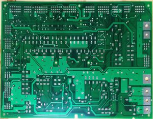
The solder mask is typically green in color, but it can be made in various colors, such as blue, red, or black. The material is usually applied in a liquid form and then cured to form a solid protective layer. However, areas where components will be soldered must remain free of solder mask to allow for proper connection. These exposed areas are referred to as solder mask openings.
What Are Solder Mask Openings?
A solder mask opening refers to the area on the PCB where the solder mask is deliberately removed to expose the underlying copper pads or traces. These openings are crucial for the assembly of components because they define the locations where soldering will occur. Without the openings, solder would not be able to reach the copper pads, and the components would not be securely attached to the PCB.
Key Functions of Solder Mask Openings:
- Allowing Soldering of Components: The most obvious purpose of solder mask openings is to provide space for soldering the component leads to the copper pads.
- Preventing Solder Bridges: Properly sized and placed openings ensure that there is enough room for the solder without allowing it to spill over to adjacent pads, preventing solder bridging.
- Improving Reliability: A well-designed solder mask and opening reduce the chances of defects such as cold solder joints, which can compromise the electrical performance of the PCB.
The Importance of Proper Solder Mask Openings
The design and placement of solder mask openings are crucial for the functionality of the PCB. Several factors come into play when determining how solder mask openings are designed:
1. Size of Solder Mask Openings
The size of the solder mask opening must be large enough to allow for proper soldering of components, but not too large that it leads to unwanted issues such as solder bridging or excessive solder paste. Generally, the size of the opening is slightly larger than the component pad to allow the solder to flow easily. However, it must also be small enough to protect adjacent pads from excessive solder.
For example, the opening should generally be around 0.2 to 0.3 mm larger than the pad size, depending on the specific requirements of the design and the type of components being soldered.
2. Placement of Solder-Mask Openings
Solder-mask openings are placed at precise locations to correspond to the copper pads where components will be mounted. Their accurate placement is essential for avoiding misalignment, which could lead to soldering problems. The placement is typically determined by the component’s footprint and the size of the pad, as well as the clearance needed between the pads to avoid accidental short circuits.
3. Clearance Requirements
There are specific clearance requirements for solder mask openings, particularly when it comes to the spacing between pads and traces. These requirements ensure that solder paste is applied properly and that there is enough room for the soldering process. The correct clearance also reduces the risk of contamination, which can lead to defects in the finished board.
Creating Solder-Mask Openings
Solder mask openings are created through the photolithography process, which is used to define the areas where the solder mask will be applied and where it will be removed. Here’s a brief overview of how the process works:
1. Designing the Solder Mask
The design of the solder mask is created in the PCB design software. During the design process, the copper pads and their associated solder mask openings are defined. The software generates a solder mask layer that is integrated with the copper layer and component layer. This layer specifies where the solder mask should remain and where the openings will be.
2. Photolithography Process
Once the PCB design is complete, the photolithography process is used to transfer the design onto the PCB. The board is coated with a photoresist layer, which is then exposed to ultraviolet (UV) light through a mask that contains the solder mask design. The unexposed areas of the photoresist are removed, leaving behind the solder mask pattern, including the openings.
3. Etching and Curing
After the solder mask pattern is transferred, the board undergoes an etching process to remove excess solder mask material. This leaves behind only the desired solder mask layer with openings over the pads. The board is then cured to harden the solder mask, ensuring that it remains firmly in place.
Challenges in Solder Mask Opening Design
Designing solder mask openings comes with its own set of challenges that manufacturers need to overcome to ensure a successful PCB assembly. Some of the common issues include:
1. Misalignment of Solder Mask Openings
Misalignment can occur during the photolithography process, which can result in the solder mask openings not being perfectly aligned with the copper pads. This misalignment can lead to poor soldering, cold solder joints, and weak electrical connections.
2. Incorrect Size of Solder Mask Openings
If the solder mask openings are too large or too small, it can lead to issues during component placement or soldering. Too small openings can prevent solder from reaching the pads, while too large openings can lead to excess solder, resulting in solder bridges or short circuits.
3. Solder Bridging and Poor Soldering
Improperly sized solder mask openings can cause solder bridging, which happens when excess solder spills over between two adjacent pads. This can create short circuits or open circuits, compromising the electrical performance of the PCB. Ensuring proper clearance between pads and adequate opening sizes helps to prevent solder bridging.
Best Practices for Designing Solder Mask-Openings
To ensure a smooth soldering process and reliable PCB assembly, the following best practices should be followed:
- Ensure Proper Solder Mask-Opening Size: The opening should be slightly larger than the copper pad to allow for proper solder flow.
- Consider Component Footprints: Ensure that the solder mask openings align with the component pads and that there is enough space to allow for accurate component placement.
- Follow Design Rules for Clearance: Maintain adequate clearance between pads and traces to prevent solder bridging and to ensure reliable solder joints.
- Test and Inspect Designs: Use Automated Optical Inspection (AOI) and other testing methods to verify the solder mask openings and overall design before fabrication.
Conclusion
Solder mask openings are an essential part of the PCB manufacturing process, ensuring that the circuit board can be populated with components and properly soldered. Correctly designed solder mask openings help ensure that the soldering process is smooth and that the final PCB performs as expected. The design, size, and placement of these openings play a vital role in the overall quality and reliability of the PCB, and adherence to best practices can significantly reduce manufacturing defects and improve the performance of the finished product. Proper solder mask opening design ensures that the electrical connections on a PCB remain strong, reliable, and free from defects that could compromise the device’s operation.

- long board pcb
- Flexible PCBs
- Special PCB
- Express Printed Circuit Board
- Pcb Prototype
- LED PCB
- PCB
- Printed Circuit Board
- Pcb meaning
- Pcb manufacturer
- Rigid pcb board
- Rigid Flex PCB
 Quote
Quote
 E-mail