1. Introduction to Rigid-Flex PCB Technology
The ever-increasing demand for miniaturized, lightweight, and multifunctional electronic devices has driven the electronics manufacturing industry to adopt more sophisticated interconnect technologies. Among these, the Rigid-Flex PCB stands out as a hybrid circuit that merges the mechanical stability of rigid boards with the design adaptability of flexible circuits. This combination enables engineers to design compact, high-performance electronic assemblies without sacrificing reliability.
1.1 What is a Rigid-Flex PCB?
A Rigid-Flex PCB (Rigid-Flexible Printed Circuit Board) is a type of multilayer circuit board that integrates both rigid and flexible substrates into a unified structure. Unlike traditional rigid boards or standalone flexible circuits, a Rigid-Flex PCB allows for dynamic bending in specific regions while maintaining rigidity in others. The flexible sections can be bent or folded during installation or service, which reduces the need for connectors and cables and enables more complex 3D configurations.
Typically, a Rigid-Flex PCB consists of multiple layers of flexible polyimide bonded to rigid FR-4 or other composite materials. The number of rigid and flexible layers can vary depending on the application requirements.
1.2 Historical Background and Market Evolution
The roots of Rigid-Flex PCB technology can be traced back to the aerospace and military sectors, where weight, space, and vibration resistance were critical constraints. Over time, the technology has expanded into consumer electronics, medical devices, industrial control systems, and automotive electronics.
In the last decade, the demand for foldable smartphones, wearable health monitors, and miniaturized imaging devices has significantly pushed the boundaries of Rigid-Flex PCB design and manufacturing. The technology continues to evolve, not only in terms of materials and stack-up configurations but also in production automation and design software integration.
1.3 Key Advantages of Rigid-Flex PCB Solutions
The adoption of Rigid-Flex PCBs offers several engineering and manufacturing advantages:
-
Compact Assembly: Eliminates bulky connectors and cabling between rigid boards, reducing overall device footprint.
-
Mechanical Reliability: Flex sections absorb shock and vibration, enhancing device longevity.
-
Design Flexibility: Enables three-dimensional packaging, which is ideal for foldable or compact devices.
-
Reduced Assembly Time and Cost: Fewer components mean fewer interconnects and less assembly labor.
-
Improved Signal Integrity: Minimizing interconnections between separate PCBs improves electrical performance and reduces EMI (electromagnetic interference).
Despite these benefits, designing and producing a Rigid-Flex PCB involves complex trade-offs in terms of mechanical stress distribution, thermal expansion, material compatibility, and cost per unit.
1.4 Typical Use Cases of Rigid-Flex PCB
Rigid-Flex PCBs are now prevalent in various sectors. Some of the most notable applications include:
-
Consumer Electronics: Foldable smartphones, cameras, smartwatches, and laptops.
-
Medical Devices: Pacemakers, hearing aids, and diagnostic imaging equipment.
-
Automotive Systems: Advanced driver-assistance systems (ADAS), infotainment units, and lighting modules.
-
Military and Aerospace: Avionics, missile guidance systems, and rugged communication devices.
-
Industrial Equipment: Robotics, automation control panels, and measurement instruments.
1.5 Strategic Perspective on the Value of Rigid-Flex PCB
From a strategic manufacturing standpoint, investing in Rigid-Flex PCB technology is not merely about adopting a trend—it’s about anticipating the trajectory of future device architectures. As IoT (Internet of Things), AI-driven wearable electronics, and edge computing proliferate, the demand for compact, reliable, and mechanically resilient electronics will only rise.
However, success in Rigid-Flex PCB implementation depends on more than just choosing the right materials or stack-ups. It requires a holistic approach encompassing co-design between electrical and mechanical engineers, close collaboration with fabrication partners, and in-depth understanding of thermal, electrical, and mechanical behavior throughout the product life cycle.
1.6 Author’s Thought: Beyond Integration—Rigid-Flex PCB as a Design Philosophy
Rather than viewing Rigid-Flex PCBs merely as a blend of rigid and flexible circuits, it’s more accurate to see them as an integrated design philosophy. They offer a unique medium where function follows form and vice versa. Engineers must think beyond two-dimensional schematics and visualize electronics spatially, understanding how circuits bend, twist, and interact under real-world constraints.
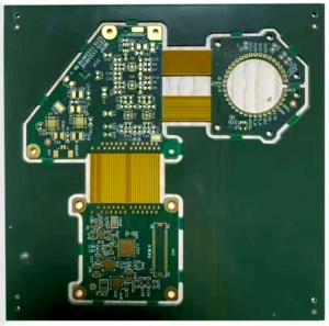
Rigid-Flex PCB
2. Rigid-Flex PCB Design Considerations and Challenges
Designing a Rigid-Flex PCB is fundamentally different from developing either a rigid or a flexible circuit independently. It requires a multidisciplinary design mindset, precise mechanical-electrical coordination, and proactive anticipation of fabrication and assembly realities. Errors at the design stage can cascade into serious yield losses, field failures, or even full product redesigns.
This section explores the core considerations and common design challenges specific to Rigid-Flex PCB systems.
2.1 Unique Design Requirements for Rigid-Flex PCB
Rigid-Flex PCBs merge rigid and flexible sections into a unified design, but this blend introduces significant complexity:
-
3D Design Integration: Designers must visualize and simulate how the flex circuits will fold or bend in the final application. This requires 3D CAD modeling, mechanical stack-up simulation, and bending radius analysis.
-
Bend Area Management: Traces and vias must avoid the dynamic bend areas unless carefully planned. Sharp corners, stubbed traces, and improper copper distribution can lead to delamination or cracking.
-
Stack-Up Planning: The choice of layer count, copper thickness, and adhesive layers directly affects electrical performance and mechanical flexibility.
A successful Rigid-Flex PCB design must incorporate these variables while balancing signal integrity, manufacturability, and mechanical durability.
2.2 CAD and EDA Tools for Rigid-Flex PCB Design
Modern Electronic Design Automation (EDA) tools have begun to support more intuitive and 3D-aware Rigid-Flex PCB design workflows. However, challenges still exist:
-
Layer Mapping and Zone Management: The software must clearly distinguish between rigid and flex zones, which can become visually and functionally complex as layer counts increase.
-
Constraint Management: Controlled impedance, bend radii, and differential pair lengths must be precisely defined and verified.
-
3D Visualization: Not all EDA tools offer realistic folding simulation, which is vital for checking mechanical interference and trace strain in bend areas.
Selecting the right tool—such as Altium Designer, Cadence Allegro, or Siemens Xpedition—can dramatically impact the effectiveness of the Rigid-Flex design process.
2.3 Signal Integrity and EMI in Rigid-Flex PCB Design
One of the key technical challenges is maintaining signal integrity across regions where the dielectric constants, trace widths, and ground referencing can vary.
-
Impedance Matching: Differential signals must maintain constant impedance across rigid and flex zones, which have different dielectric characteristics.
-
Return Path Planning: Poor ground continuity through bend zones can create noise loops and EMI issues.
-
Stub Elimination: Because flexible traces can be long and narrow, avoiding stubs or unterminated ends becomes crucial for high-speed signals.
These concerns make pre-layout simulation and post-layout verification using tools like HyperLynx or Sigrity an essential part of Rigid-Flex PCB design.
2.4 Mechanical Stress and Bend Radius Management in Rigid-Flex PCB
In flexible areas, mechanical stress is a dominant design factor:
-
Minimum Bend Radius: Exceeding the manufacturer-recommended bend radius can result in trace cracking or delamination. For dynamic flexing, larger bend radii are required compared to static folds.
-
Trace Routing Strategy: Traces should be routed perpendicular to the bend direction and staggered between layers to distribute stress evenly.
-
Component Placement: No components or vias should be placed in the bend areas, as these are subject to repetitive mechanical stress during folding or device movement.
Understanding mechanical deformation and fatigue behavior is as important as electrical considerations when designing a Rigid-Flex PCB.
2.5 DFM and DFA Constraints in Rigid-Flex PCB
Design for Manufacturability (DFM) and Design for Assembly (DFA) principles become more critical when rigid and flex sections are combined:
-
Tooling Holes and Fiducials: These must be aligned precisely across rigid and flex sections for proper registration during fabrication.
-
Panelization Strategy: The irregular shapes of Rigid-Flex PCBs may require creative panelization techniques to optimize material use and yield.
-
Solder Joint Stability: Thermal expansion mismatch between rigid and flex regions can affect component solder joints near the transitions.
Ignoring these constraints during the design phase may lead to re-spins or manufacturing delays.
2.6 Documentation and Communication with Fabricators
Because of the intricate nature of Rigid-Flex designs, thorough documentation is critical:
-
Layer Stack-Up Tables: Must clearly distinguish between rigid, flex, and adhesive layers.
-
Bend Instructions: Fold sequences, direction of flexing, and number of cycles expected must be communicated.
-
Material Specifications: Detailed call-outs for coverlay, stiffeners, flex materials, adhesives, and surface finishes.
It is advisable to involve the PCB fabricator early during the design stage to validate design assumptions and align expectations, especially regarding manufacturing tolerances and capabilities.
3. Material Selection in Rigid-Flex PCB Fabrication
Material selection is one of the most decisive factors in the performance, reliability, and cost of a Rigid-Flex PCB. Given that these hybrid boards must operate across rigid and bendable regions, each layer and substrate must meet stringent electrical, thermal, and mechanical criteria. The mismatch or misapplication of materials can lead to warping, delamination, electrical failure, or unmanufacturable designs.
This section explores the critical materials used in Rigid-Flex PCB fabrication, their properties, selection strategies, and real-world implications.
3.1 Role of Base Materials in Rigid-Flex PCB Performance
The base materials used in both the rigid and flex sections dictate the core physical behaviors of the final PCB. These include:
-
Dimensional stability during temperature cycling or flexing
-
Dielectric properties for high-frequency performance
-
Thermal resistance to withstand soldering and environmental stress
-
Adhesion and bonding compatibility between rigid and flexible sections
Each functional layer—conductor, substrate, adhesive, and coverlay—must be selected with system-level trade-offs in mind.
3.2 Flexible Core Materials for Rigid-Flex PCB
The flexible regions of a Rigid-Flex PCB typically use polyimide as the dielectric base due to its superior thermal resistance, chemical durability, and mechanical flexibility.
Key flexible core materials include:
-
Polyimide Film (e.g., Kapton)
-
Excellent thermal resistance (>250°C)
-
Low dielectric constant (≈3.5)
-
Highly resistant to cracking under flex stress
-
-
Adhesiveless Polyimide Laminates
-
Provide thinner profiles and higher dimensional stability
-
Recommended for fine-line HDI Rigid-Flex designs
-
-
LCP (Liquid Crystal Polymer) – Emerging in high-frequency designs
-
Low moisture absorption
-
Stable dielectric behavior at GHz frequencies
-
More expensive and less flexible than polyimide
-
Material decisions in flex regions must account for bend radius, flex life cycle (dynamic vs static), and the required thermal budget.
3.3 Rigid Core and Prepreg Materials in Rigid-Flex PCB
The rigid sections usually employ standard FR-4 epoxy-glass laminates. However, in high-reliability or high-speed environments, alternative materials may be necessary:
-
Standard FR-4 (Tg ≈ 135°C)
-
Suitable for consumer-grade electronics
-
Cost-effective, but limited thermal and electrical stability
-
-
High-Tg FR-4 (Tg > 170°C)
-
Recommended for lead-free soldering profiles
-
Reduces risk of delamination and CAF (conductive anodic filamentation)
-
-
Polyimide-Based Rigid Laminates
-
Higher thermal endurance for aerospace and defense
-
Slightly more expensive and harder to process
-
-
Rogers or Megtron for RF Performance
-
Used in Rigid-Flex PCBs with controlled impedance and high-speed data paths
-
It is crucial that the rigid core materials bond effectively with adjacent flexible layers and do not induce stress during lamination.
3.4 Adhesives and Bonding Films in Rigid-Flex PCB Construction
The interfacial bond between rigid and flex sections must be strong enough to endure repeated mechanical and thermal stress. Adhesives are used to laminate layers and secure flexible circuits inside rigid stack-ups.
Common adhesives include:
-
Acrylic-Based Adhesives
-
Easy to process
-
Good chemical resistance but lower thermal stability
-
-
Epoxy-Based Adhesives
-
Superior thermal endurance
-
Prone to brittleness if not formulated correctly
-
-
Modified Polyimide Adhesives
-
Ideal for military and aerospace Rigid-Flex PCB systems
-
High reliability and stable across wide temperature ranges
-
The adhesive system must be compatible with reflow profiles, flexing stress, and humidity exposure over the product’s lifetime.
3.5 Copper Foils and Conductor Types in Rigid-Flex PCB
Copper conductors are the lifelines of any PCB. In Rigid-Flex PCB fabrication, choosing the correct type and thickness of copper is crucial for flexibility and etch precision.
Options include:
-
Rolled Annealed (RA) Copper
-
Preferred for dynamic flex regions due to grain orientation
-
Better bend resistance compared to electro-deposited copper
-
-
Electro-Deposited (ED) Copper
-
Used in rigid sections for cost-effectiveness
-
Less suitable for repeated flexing
-
-
Double-Treat Copper Foils
-
Provide better adhesion in bonding layers
-
Copper thickness is also a balancing act: thick copper improves current-carrying capacity but increases stiffness and minimum bend radius.
3.6 Coverlay vs Solder Mask in Rigid-Flex PCB
The outermost layer on the flexible sections is typically coverlay, not traditional solder mask. Coverlay is made of polyimide and adhesive layers that protect the copper circuitry from oxidation and mechanical damage.
Coverlay properties:
-
Withstands repeated flexing
-
Provides excellent dielectric insulation
-
Must be laser- or mechanically-cut for pad exposure
In contrast, liquid photoimageable (LPI) solder mask is used for rigid sections. Improper use of solder mask in flex regions can lead to cracking or delamination during bending.
3.7 Stiffeners and Reinforcements in Rigid-Flex PCB
Stiffeners are used to mechanically support connectors, components, or mounting holes placed near or on the flex areas. Material choices include:
-
FR-4 stiffeners – For low-cost mechanical support
-
PI (polyimide) stiffeners – For thin-profile areas
-
Steel or aluminum stiffeners – For high-strength or heat-dissipating needs
The placement of stiffeners must align with assembly requirements while avoiding stress concentrations.
3.8 Moisture Sensitivity and Outgassing Considerations
Moisture absorption in flex materials can cause delamination, blistering, or outgassing during high-temperature processes like reflow soldering. As such, materials must be:
-
Low in moisture absorption (<0.1% preferred)
-
Properly pre-baked before lamination and assembly
-
Selected based on their thermal expansion characteristics (CTE)
A mismatch in CTE between layers can introduce mechanical fatigue, especially after many thermal cycles.
4. Layer Stack-Up Strategy for Rigid-Flex PCB
A well-designed layer stack-up is the structural backbone of any Rigid-Flex PCB. Unlike traditional rigid boards where layers are uniform across the entire board area, Rigid-Flex PCBs involve variable stack-ups across rigid and flexible regions. This variability introduces added complexity—but also empowers compact, high-functioning electronic systems.
In this section, we delve into the fundamentals, strategies, and advanced considerations behind building an optimal layer stack-up for a Rigid-Flex PCB.
4.1 The Purpose of Stack-Up Planning in Rigid-Flex PCB
Stack-up planning is not just about defining copper and dielectric layers; it directly impacts:
-
Electrical performance, especially impedance and signal return paths
-
Mechanical reliability, such as bend tolerance and flex durability
-
Thermal behavior, particularly with heat dissipation across dense circuitry
-
Manufacturability, since fabrication steps like drilling, lamination, and imaging rely on the defined structure
In Rigid-Flex PCB design, the stack-up defines what layers are rigid, what layers are flex, how they transition, and how many times the flex regions cross through rigid sections.
4.2 Common Stack-Up Configurations for Rigid-Flex PCB
Here are some widely used stack-up structures:
a) Type 1: Single-Layer Flex with Double-Sided Rigid
-
Simple and cost-effective
-
Flex layer connects two rigid boards
-
Suitable for static flex applications (e.g., fold-only once)
b) Type 2: Double-Layer Flex with Rigid Cores
-
Two flex layers with ground/power planes
-
Enhanced EMI control
-
Suitable for semi-dynamic bending
c) Type 3: Multi-Layer Rigid-Flex
-
Multiple flex layers with complex signal routing
-
Rigid areas can house components on multiple layers
-
Ideal for high-density, foldable designs (e.g., wearables, imaging devices)
Each configuration must be carefully simulated and validated for both electrical performance and mechanical tolerances.
5. Drilling and Via Formation in Rigid-Flex PCB Manufacturing
The drilling and via formation process is a critical stage in Rigid-Flex PCB manufacturing. Vias serve as interlayer electrical connections between copper layers in both the rigid and flexible zones. Given the hybrid structure of rigid-flex boards, the requirements for hole types, drill quality, and via reliability are significantly more complex than in standard rigid PCBs.
This section explores the various types of holes, their formation techniques, and key considerations unique to Rigid-Flex PCB designs.
5.1 Importance of Drilling in Rigid-Flex PCB Fabrication
Drilled vias in Rigid-Flex PCBs serve three essential purposes:
-
Electrical Interconnection: Connecting signal and power layers across rigid and/or flex sections
-
Mechanical Alignment: Ensuring registration between layers during lamination
-
Assembly Functionality: Enabling component leads and press-fit connectors to be inserted
Due to multiple lamination cycles and varying material properties between rigid and flexible sections, achieving precise, clean hole structures is essential for overall board integrity and performance.
5.2 Types of Holes in Rigid-Flex PCB
A wide variety of hole types are used in Rigid-Flex PCB builds, each with specific functions and fabrication challenges:
-
Through-Hole Vias:
Pass completely through the entire PCB stack. Common in both rigid and flex areas but must be carefully managed to avoid stress points in bendable regions. -
Blind Vias:
Connect outer layers to inner layers without going through the entire board. Used for high-density routing in rigid sections. -
Buried Vias:
Connect inner layers only, invisible from the outer surfaces. Useful in multilayer rigid areas to free up surface space. -
Microvias:
Small-diameter (typically <150 µm) vias used in HDI (High Density Interconnect) Rigid-Flex PCBs. Laser drilled, often in rigid layers only. -
Backdrilled Vias:
Remove unused via stubs to reduce signal reflection in high-speed circuits. Usually applicable in high-frequency Rigid-Flex designs. -
Component Holes:
Larger mechanical holes for component leads, connectors, or mounting hardware.
5.3 Mechanical Drilling in Rigid-Flex PCB Manufacturing
Mechanical drilling remains the most common method for creating larger via holes and component holes:
-
Carbide Drill Bits are used for precision drilling through multiple layers.
-
Spindle speeds and feed rates must be finely tuned, especially when drilling through soft materials like polyimide and adhesives.
-
Drill wander is a concern due to varying material densities in rigid-flex zones, particularly near the rigid-to-flex transition.
Drill quality can be affected by:
-
Delamination at hole entry/exit points
-
Resin smear in adhesive layers
-
Burr formation on copper edges
To reduce mechanical stress, flex regions are often drilled in pre-lamination stages or selectively reinforced.
5.4 Laser Drilling of Microvias in Rigid-Flex PCB
Laser drilling is essential for microvias and blind vias in HDI Rigid-Flex PCB designs. UV or CO₂ lasers are typically used, depending on the target material.
Benefits of laser drilling:
-
High precision for fine-feature via structures
-
Selective drilling of flex-only or rigid-only zones
-
Minimal mechanical stress, which is ideal for fragile dielectric materials
However, challenges exist:
-
Polyimide absorbs laser energy differently than FR-4, leading to non-uniform hole shapes
-
Debris removal and sidewall cleanliness must be managed post-drilling
-
Adhesive and coverlay residues can accumulate in drilled areas, requiring plasma cleaning
5.5 Plating and Metallization of Vias in Rigid-Flex PCB
After drilling, vias must be metallized to create conductive paths between layers:
-
Desmear Process:
Chemical or plasma treatments remove resin smear and improve adhesion. -
Electroless Copper Deposition:
Deposits a thin conductive layer inside the hole walls. -
Electrolytic Copper Plating:
Builds up copper thickness to meet electrical and mechanical reliability standards.
In Rigid-Flex PCB, special attention is needed because flex materials absorb chemicals differently, and plating uniformity is harder to control across mixed dielectric stacks.
5.6 Via Reliability and Failure Modes in Rigid-Flex PCB
Via reliability is a major concern, especially across thermal cycling and mechanical stress. Common failure modes include:
-
Barrel Cracking:
Caused by expansion/contraction mismatch between plated copper and base material. -
Corner Cracking at Rigid-Flex Transition:
Occurs when vias are placed too close to the interface of rigid and flexible zones. -
Void Formation in Plating:
Results from poor surface preparation or inconsistent copper growth. -
Delamination Around Hole Walls:
Especially common in stacked laminations or excessive drilling pressure.
To mitigate these risks, Rigid-Flex PCB manufacturers must use optimized plating parameters, stress testing, and X-ray inspection during production.
5.7 Design Guidelines for Via Placement in Rigid-Flex PCB
Good via placement strategy is crucial for mechanical durability:
-
Avoid placing vias in dynamic flex areas. Instead, restrict them to static or reinforced flex zones.
-
Keep vias away from bend lines, especially in Z-fold or U-bend configurations.
-
Use teardrop-shaped pads to relieve mechanical stress at hole edges.
-
Stagger vias between layers when stacking is unavoidable, to reduce via barrel fatigue.
Where high-density routing is necessary in flexible regions, consider via-in-pad designs, but only after consultation with the fabricator due to process complexity.
Conclusion: The Future and Importance of Rigid-Flex PCB Manufacturing
Rigid-Flex PCB manufacturing represents a sophisticated fusion of rigid and flexible circuit technologies, enabling innovative electronic solutions that demand compactness, durability, and versatility. Throughout this comprehensive fabrication guide, we have explored every critical phase—from material selection, etching, lamination, and coverlay application, to surface finishing, testing, and design considerations—each uniquely tailored to the complex nature of rigid-flex circuits.
Key takeaways include:
-
Material Compatibility and Process Control: The hybrid nature of rigid and flexible substrates requires meticulous attention to materials and process parameters to ensure integrity and performance.
-
Precision in Fabrication: Techniques such as controlled etching, multi-stage lamination, and accurate coverlay application are vital to achieve the mechanical flexibility and electrical reliability that rigid-flex PCBs demand.
-
Testing and Quality Assurance: Robust electrical, mechanical, and environmental testing protocols safeguard the long-term functionality of these advanced circuits.
-
Design Collaboration: Early integration of design and manufacturing knowledge minimizes risks, reduces costs, and enhances manufacturability.
-
Embracing Emerging Technologies: Innovations in materials, laser processing, embedded components, and smart manufacturing are driving the evolution of rigid-flex PCB capabilities.
Reflecting on this journey, rigid-flex PCB manufacturing is both a science and an art—a careful balance of chemistry, mechanics, and electronics, all converging to meet the challenging demands of modern devices. Its role in advancing technology across industries like aerospace, medical devices, consumer electronics, and automotive is indispensable.
As the field continues to advance, professionals involved must remain agile, continuously learning and adapting to new materials, processes, and design paradigms. Only through such dedication can the full potential of rigid-flex PCBs be realized, shaping the future of electronic innovation.

- long board pcb
- Flexible PCBs
- Special PCB
- Express Printed Circuit Board
- Pcb Prototype
- LED PCB
- PCB
- Printed Circuit Board
- Pcb meaning
- Pcb manufacturer
- Rigid pcb board
- Rigid Flex PCB
 Quote
Quote
 E-mail