Portel PCB: A Comprehensive Guide to PCB Design with Portel Software
Introduction
Portel PCB is a widely used printed circuit board (PCB) design software that provides powerful tools for designing, simulating, and manufacturing PCBs. The software is known for its efficiency in handling complex PCB layouts, high-speed signal routing, and design validation. In this article, we will explore the features, benefits, applications, and workflow of Portel PCB, along with best practices for designing high-quality PCBs.
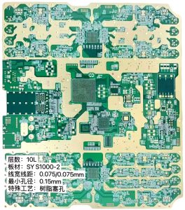
blank circuit board Portel PCB
What is Portel PCB?
Portel PCB is a professional PCB design software that enables engineers to create schematic diagrams, design PCB layouts, and generate Gerber files for manufacturing. It is used by professionals in industries such as consumer electronics, automotive, aerospace, and industrial automation.
The software integrates multiple tools for circuit simulation, component management, and rule-based design, ensuring high accuracy and reliability in PCB development.
Key Features of Portel PCB
1. Schematic Capture
Portel PCB provides an intuitive schematic capture tool that allows engineers to create and edit circuit diagrams. The schematic editor supports:
- Drag-and-drop component placement
- Electrical rule checking (ERC)
- Netlist generation for PCB layout
2. PCB Layout and Routing
The software includes a powerful PCB editor that supports:
- Multi-layer PCB design
- Automatic and manual routing options
- High-speed signal routing
- Design rule checking (DRC) to prevent errors
3. Component Library Management
Portel PCB comes with an extensive component library, including:
- Pre-built electronic components
- Customizable footprints and symbols
- Integration with online component databases
4. 3D Visualization and Design Simulation
Portel PCB enables real-time 3D visualization, allowing engineers to:
- Check component placement and alignment
- Simulate circuit behavior before manufacturing
- Detect potential design flaws early
5. Gerber File Generation
The software automatically generates Gerber files, the industry-standard format for PCB manufacturing, ensuring seamless communication between designers and manufacturers.
Benefits of Using Portel PCB
1. High Design Accuracy
With advanced ERC and DRC tools, engineers can minimize errors and ensure circuit integrity.
2. Faster Prototyping
Portel PCB’s streamlined workflow accelerates the prototyping process, reducing development time and costs.
3. Improved Signal Integrity
The software supports high-speed routing techniques and signal integrity analysis, making it ideal for RF and high-frequency PCB designs.
4. Seamless Collaboration
Portel PCB integrates with cloud platforms, enabling multiple engineers to work on the same project efficiently.
5. Support for High-Density Designs
With multi-layer PCB support and HDI routing capabilities, Portel PCB allows for compact and high-performance PCB designs.
Applications of Portel PCB
Portel PCB is used in various industries, including:
1. Consumer Electronics
- Smartphones, tablets, and wearable devices
- Home automation and IoT devices
2. Automotive Electronics
- Engine control modules (ECUs)
- Advanced driver assistance systems (ADAS)
- In-vehicle infotainment systems
3. Aerospace and Defense
- Avionics systems
- Military-grade communication equipment
- Radar and surveillance systems
4. Medical Devices
- Diagnostic equipment
- Patient monitoring systems
- Implantable medical devices
5. Industrial Automation
- Robotics and motion control systems
- Power management circuits
- Factory automation and monitoring systems
Workflow of PCB Design Using Portel PCB
Step 1: Schematic Design
- Select components from the library
- Connect components using wires and buses
- Perform electrical rule checks
- Generate a netlist for PCB layout
Step 2: PCB Layout Design
- Import the schematic netlist into the PCB editor
- Define board dimensions and layer stack-up
- Place components manually or use auto-placement tools
- Route signal traces using manual or auto-routing options
- Perform design rule checks (DRC) to detect any violations
Step 3: Signal Integrity and Thermal Analysis
- Analyze high-speed signals and impedance matching
- Check thermal dissipation and heat sink requirements
- Optimize trace width and spacing for EMI/EMC compliance
Step 4: 3D Visualization and Verification
- Review the PCB layout in 3D mode
- Ensure proper component clearance and alignment
- Detect mechanical interferences
Step 5: Gerber File Export and Manufacturing Preparation
- Generate Gerber files, drill files, and BOM (Bill of Materials)
- Validate files using a Gerber viewer
- Send the design for PCB fabrication and assembly
Best Practices for Designing PCBs with Portel PCB
1. Follow Standard Design Rules
- Use appropriate trace width and spacing for signal integrity
- Define correct pad sizes and via types
- Ensure proper grounding and power distribution
2. Optimize Component Placement
- Place high-speed components close to the controller
- Minimize trace lengths to reduce signal loss
- Group related components logically for easier routing
3. Use Proper Layer Stack-Up
- For multi-layer PCBs, separate power and ground layers
- Avoid excessive via stacking to prevent signal interference
4. Perform Thorough Design Validation
- Run DRC and ERC before finalizing the layout
- Use simulation tools to detect potential issues
- Verify thermal management strategies for high-power circuits
5. Check Manufacturing Constraints
- Ensure minimum drill hole sizes match manufacturer capabilities
- Define solder mask and silkscreen layers correctly
- Generate accurate Gerber files for fabrication
Future Trends in PCB Design with Portel PCB
1. AI-Assisted PCB Design
- Automated component placement and routing
- Predictive error detection and optimization
2. Integration with IoT and Cloud Platforms
- Real-time design collaboration across teams
- Cloud-based component libraries and version control
3. Advanced Materials and Miniaturization
- Use of flexible and stretchable PCBs
- Higher-density HDI (High-Density Interconnect) designs
4. Improved Simulation and Testing Tools
- Enhanced SPICE simulations for analog circuits
- Integrated thermal and EMI analysis
Conclusion
Portel PCB is a powerful and versatile PCB design tool that provides a comprehensive solution for schematic design, PCB layout, simulation, and manufacturing preparation. With its advanced routing capabilities, signal integrity analysis, and extensive component libraries, Portel PCB is widely used in industries ranging from consumer electronics to aerospace and medical devices.
By following best practices and leveraging the latest innovations in PCB design, engineers can develop high-performance, reliable, and manufacturable electronic products using Portel PCB. As technology evolves, the integration of AI, cloud collaboration, and advanced simulation tools will further enhance PCB design efficiency and innovation.

- long board pcb
- Flexible PCBs
- Special PCB
- Express Printed Circuit Board
- Pcb Prototype
- LED PCB
- PCB
- Printed Circuit Board
- Pcb meaning
- Pcb manufacturer
- Rigid pcb board
- Rigid Flex PCB
 Quote
Quote
 E-mail