PCB Stencil Thickness: Importance, Selection, and Best Practices
Introduction
PCB stencil thickness plays a crucial role in the Surface Mount Technology (SMT) assembly process, directly affecting solder paste deposition, component placement accuracy, and overall soldering quality. Choosing the right stencil thickness ensures optimal solder joint reliability and minimizes defects such as solder bridging, insufficient solder, and tombstoning.
This article explores the importance of PCB stencil thickness, how to select the right thickness for different PCB designs, key influencing factors, and best practices to achieve high-quality PCB assembly.
pcb stencil thickness
What is PCB Stencil Thickness?
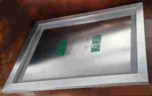
A PCB stencil is a thin metal sheet, usually made of stainless steel, used in the solder paste printing process for SMT assembly. The stencil has precisely cut apertures that align with PCB pads, allowing solder paste to be accurately deposited onto the board before placing surface mount components.
The thickness of the PCB stencil determines the amount of solder paste applied to the PCB pads. It is measured in micrometers (µm) or mils (1 mil = 0.001 inches). Common stencil thickness values range from 0.08mm (3 mils) to 0.20mm (8 mils), depending on PCB design complexity, component types, and manufacturing requirements.
Why PCB Stencil Thickness Matters
The stencil thickness directly impacts several key factors in SMT assembly:
1. Solder Paste Volume Control
- Thicker stencils allow more solder paste deposition, which is beneficial for large components such as power devices and connectors.
- Thinner stencils reduce solder paste volume, preventing excessive solder that can cause bridging or short circuits.
2. Component Placement Accuracy
- Too much solder paste can cause misalignment and uneven placement of components.
- Proper stencil thickness ensures precise solder paste printing, leading to stable and reliable component positioning.
3. Avoiding Defects in Soldering
- Excess solder paste can lead to solder bridging (short circuits between pads).
- Insufficient solder paste can cause cold solder joints, leading to poor electrical connectivity or mechanical weakness.
- Optimal stencil thickness prevents tombstoning (one side of a component lifting during reflow).
4. Compatibility with Fine-Pitch Components
Fine-pitch components (such as BGA, QFN, and 0201-sized chips) require a thin stencil to ensure precise solder paste application. A stencil that is too thick can cause excessive paste deposition, leading to bridging and reflow issues.
Common PCB Stencil Thickness Options
The optimal stencil thickness depends on the PCB design, component types, and pad sizes. Below is a guideline for choosing stencil thickness based on component pitch:
| Stencil Thickness | Component Type & Pitch | Application |
|---|---|---|
| 0.08mm (3 mils) | Fine-pitch (0.3mm BGA, 0201 components) | High-density PCBs, HDI boards |
| 0.10mm (4 mils) | Fine-pitch QFP, 0402, small BGAs | Mobile devices, wearables |
| 0.12mm (5 mils) | General SMT (0603, QFP, small power components) | Standard PCBs |
| 0.15mm (6 mils) | Mixed components (QFP, BGA, power components) | Industrial and automotive PCBs |
| 0.20mm (8 mils) | Large pads (connectors, power ICs, LED PCBs) | High-power electronics |
For mixed-technology PCBs, where fine-pitch and large components coexist, a step stencil (with varying thickness areas) may be used to balance solder paste deposition.
Factors Affecting PCB Stencil Thickness Selection
Several factors influence the choice of PCB stencil thickness:
1. Component Size and Pitch
- Fine-pitch components require a thinner stencil for precise paste application.
- Large power components or through-hole components (THT) need thicker stencils for adequate solder volume.
2. PCB Pad Design and Spacing
- Narrow pad spacing demands a thinner stencil to prevent excess solder.
- Wider pad spacing allows the use of thicker stencils without risking solder bridges.
3. Stencil Aperture Design
- Aperture size-to-thickness ratio (Aspect Ratio) should be carefully calculated.
- A ratio of 1.5 or higher ensures good solder paste release.
4. Solder Paste Type
- Type 3 or Type 4 solder pastes are commonly used for standard PCBs.
- Type 5 or finer solder pastes work better with thinner stencils for ultra-fine-pitch applications.
5. PCB Application and Assembly Requirements
- High-reliability applications (medical, aerospace) require tight control over solder paste volume.
- LED PCBs and power boards benefit from thicker stencils to ensure sufficient solder.
Best Practices for PCB Stencil Thickness Selection
To achieve optimal SMT assembly results, follow these best practices when selecting and using PCB stencils:
✔ Consult IPC-7525 Standards: Follow industry standards for stencil design and thickness selection.
✔ Use Step Stencils for Mixed Components: For PCBs with both fine-pitch and large components, consider using step stencils with variable thickness to balance solder paste volume.
✔ Optimize Aperture Design: Use rounded corners in stencil apertures to improve paste release. Reduce aperture size slightly for fine-pitch pads to control solder volume.
✔ Choose Laser-Cut Stencils: Laser-cut stainless steel stencils offer better precision and paste release compared to chemically etched stencils.
✔ Regularly Inspect and Clean Stencils: Ensure proper solder paste deposition by cleaning stencils regularly to prevent clogged apertures.
✔ Test Before Mass Production: Perform solder paste printing tests and adjust stencil thickness if needed to optimize reflow soldering results.
Conclusion
Selecting the right PCB stencil thickness is critical for ensuring high-quality solder joints, defect-free assembly, and reliable PCB performance. By understanding the impact of stencil thickness on solder paste volume, component placement, and soldering defects, manufacturers can optimize their SMT processes for different PCB designs.
For fine-pitch components, thinner stencils (0.08mm–0.12mm) provide precise solder paste control, while larger components and power applications require thicker stencils (0.15mm–0.20mm) for sufficient solder volume.
By following industry best practices, proper aperture design, and stencil maintenance, manufacturers can improve yield rates, reduce defects, and enhance the overall reliability of PCB assemblies.
If you are looking for high-precision PCB stencils for your SMT assembly, Shuoqiang Electronics offers custom stencil fabrication with laser-cut accuracy to meet your manufacturing needs. Contact us today for professional PCB solutions!

- long board pcb
- Flexible PCBs
- Special PCB
- Express Printed Circuit Board
- Pcb Prototype
- LED PCB
- PCB
- Printed Circuit Board
- Pcb meaning
- Pcb manufacturer
- Rigid pcb board
- Rigid Flex PCB
 Quote
Quote
 E-mail