PCB Slip Rings: Definition and Core Principles
Printed Circuit Board (PCB) Slip Rings are an advanced type of rotary electrical connector that leverage the architecture of PCBs to provide continuous electrical connections between stationary and rotating parts of a system. Unlike traditional slip rings that rely on bulky wire-wound structures and carbon brush contacts, PCB Slip Rings make use of flat, planar conductive paths etched into multilayer boards. These conductive tracks are carefully designed to maintain consistent contact with rotating brush assemblies, ensuring that power and signals can pass seamlessly through the rotating interface.
In essence, a PCB Slip Ring acts as a bridge for electrical signals in systems where rotation and compact size are critical. They combine the mechanical rotation of slip rings with the precision manufacturing and layout capabilities of PCBs. This unique approach significantly reduces size, weight, and assembly complexity, making them ideal for modern compact systems such as drones, medical imaging equipment, and advanced robotics.
Another way to understand PCB Slip Rings is to compare them to highways. In a conventional slip ring, the path for electricity is like a winding, uneven rural road—functional but prone to wear and disruption. In contrast, the conductive tracks of PCB Slip Rings are like well-planned multilane highways: smoother, more reliable, and capable of handling higher speeds without interruptions. This analogy highlights the sophistication of the technology.
From my perspective, the greatest contribution of PCB Slip Rings lies in their ability to merge two historically separate engineering disciplines—mechanical rotation and advanced PCB fabrication—into one cohesive solution. It is this integration that truly simplifies design for engineers and saves critical space inside modern devices.
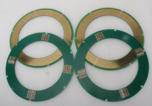
PCB Slip Ring
PCB Slip Rings: Construction and Working Mechanism
The construction of PCB Slip Rings begins with multilayer printed circuit boards, typically designed with alternating conductive and insulating layers. The conductive layers are etched to form circular tracks and pads. These rings serve as the pathways for electrical signals. Each track is carefully dimensioned to optimize current-carrying capacity, minimize crosstalk, and ensure low resistance.
A brush assembly—often made of precious metals such as gold or silver alloys—maintains physical contact with the tracks while the board rotates. Because the contact is distributed over flat, wide surfaces instead of narrow wires, the wear rate is lower, and the electrical connection remains more stable over time.
Key features of the working mechanism include:
-
Rotational Interface: The stationary brushes press gently against the PCB’s conductive rings, enabling uninterrupted transmission.
-
Low Friction: The planar surface reduces mechanical wear, extending lifespan.
-
Multichannel Capability: Multiple concentric rings on a single PCB can carry signals and power simultaneously.
-
High-Frequency Support: Flat conductive paths are more suitable for high-frequency data, which is critical for modern communication systems.
An interesting point is how this design allows engineers to scale complexity. For instance, by adding more layers to the PCB, designers can integrate dozens or even hundreds of channels into one compact slip ring. This would be nearly impossible with conventional designs due to space and manufacturing constraints.
In my observation, the elegance of PCB Slip Rings is not just in their technical advantages but in their manufacturability. Because they rely on established PCB fabrication processes, they benefit from the maturity of the PCB industry: precise etching, multilayer stacking, and automated testing. This synergy reduces cost and accelerates development cycles.
PCB Slip Rings: Advantages in Compact Design
One of the most celebrated advantages of PCB Slip Rings is their ability to drastically reduce the space required for rotary connections. Traditional slip rings are often cylindrical and bulky, consuming precious room in systems where every millimeter matters. PCB Slip Rings, by contrast, are flat and compact, allowing them to be integrated into tight spaces such as gimbals, endoscopic devices, and satellite payloads.
The space-saving aspect comes from two characteristics:
-
Planar Geometry: The slip ring’s flat disc structure can be stacked within systems without interfering with other components.
-
Integration Capability: Because they share the same fabrication techniques as other PCB modules, they can sometimes be merged directly into the main system PCB, eliminating the need for a separate component altogether.
This compactness translates into broader design freedom. Engineers are no longer forced to compromise between rotational capability and available space. For example, in small consumer drones, PCB Slip Rings enable the smooth transmission of video signals from rotating cameras without adding bulky mechanisms.
From my point of view, this integration reflects a broader trend in electronics: the push towards miniaturization without sacrificing performance. Just as microchips allowed thousands of transistors to fit on a tiny silicon wafer, PCB Slip Rings allow dozens of channels to be transmitted in a slim, planar format. This is why they are increasingly favored in cutting-edge designs.
PCB Slip Rings: Performance and Reliability Advantages
Apart from space savings, PCB Slip Rings offer significant performance and reliability improvements compared to conventional slip rings.
-
Durability and Longevity: The wide surface area contact reduces localized wear. As a result, PCB Slip Rings often last millions of rotational cycles with minimal maintenance.
-
Low Electrical Noise: Because of smoother contact surfaces and optimized conductive paths, they exhibit far less signal distortion. This is especially important in high-speed data transmission such as HD video or radar signals.
-
Stable Impedance: The etched copper paths on PCBs allow precise control over impedance, a critical factor in high-frequency signal integrity.
-
Low Profile and Weight: The lightweight structure makes them ideal for aerospace and portable devices.
-
Scalability: Engineers can easily design PCB Slip Rings with additional layers for more channels without significantly increasing the form factor.
A practical example can be seen in medical imaging machines such as CT scanners. These devices rotate rapidly while transmitting massive amounts of imaging data. PCB Slip Rings not only ensure stable, noise-free transmission but also reduce downtime due to their longer service life.
In my analysis, the long-term cost savings from improved reliability are often underestimated. While initial costs may be comparable or slightly higher than traditional slip rings, the reduction in maintenance, downtime, and replacement parts makes PCB Slip Rings far more economical over the lifetime of a device.
PCB Slip Rings: Cost and Manufacturing Efficiency
Cost efficiency is another decisive benefit. Because PCB Slip Rings leverage existing PCB manufacturing infrastructure, they are produced with a high degree of automation and precision. This results in lower per-unit costs when produced at scale.
Manufacturing advantages include:
-
High repeatability and consistency.
-
Possibility of integrating test points directly into the slip ring design.
-
Reduced manual labor compared to hand-assembled wire-based slip rings.
Moreover, the total cost of ownership is much lower. Reduced maintenance, fewer replacements, and minimal downtime all contribute to significant savings. For industrial automation companies, this translates into more predictable operational expenses and higher equipment uptime.
From my perspective, the manufacturing synergy is what makes PCB Slip Rings not just a technological improvement but also an economically viable solution. It is this dual benefit—better performance at competitive cost—that ensures their growing adoption.
PCB Slip Rings: Applications in Consumer Electronics
One of the most visible arenas where PCB Slip Rings are making a difference is in consumer electronics. Modern consumer devices are shrinking in size yet expanding in functionality, a trend that aligns perfectly with the advantages offered by PCB Slip Rings.
1. Wearable Devices
Smartwatches, fitness trackers, and AR/VR headsets often integrate rotating components such as miniature cameras or sensor modules. Traditional slip rings would be impractical due to their bulk, but PCB Slip Rings provide the necessary rotational connection in an ultra-compact footprint. The flat geometry also makes it easier to design sleek, lightweight devices without compromising durability.
2. Smart Cameras and Gimbals
Stabilized cameras used in drones or handheld gimbals depend on uninterrupted signal transmission from rotating cameras to the control board. PCB Slip Rings ensure smooth power delivery and high-speed video transmission without adding noticeable weight. This has been particularly beneficial for aerial drones, where every gram saved contributes to longer flight time.
3. Gaming and Virtual Reality Systems
Rotating interfaces in VR headsets benefit greatly from PCB Slip Rings because they support high-bandwidth data channels necessary for immersive experiences. This reduces lag and improves user comfort.
From my point of view, the role of PCB Slip Rings in consumer electronics represents a subtle but powerful shift: end-users rarely notice the technology, yet their experience of fluid movement, uninterrupted data, and device compactness depends heavily on it.
PCB Slip Rings: Applications in Medical Devices
Medical technology demands not only precision but also reliability and compactness. PCB Slip Rings meet all these requirements.
1. Surgical Robots
Robotic-assisted surgery involves highly articulated arms with multiple joints, many of which require continuous power and signal rotation. PCB Slip Rings allow these joints to rotate freely while maintaining stable connections for control signals, cameras, and haptic feedback systems.
2. Imaging Equipment
Devices such as CT and MRI scanners require the rotation of large imaging arrays around patients. PCB Slip Rings handle the massive data throughput while ensuring stable power supply to sensors. The reduced wear and long lifespan are crucial for minimizing downtime in hospital environments.
3. Portable Diagnostic Devices
Compact diagnostic machines used in fieldwork or point-of-care settings benefit from the space efficiency of PCB Slip Rings. They allow engineers to build devices that are both powerful and portable.
In my analysis, the adoption of PCB Slip Rings in medical technology goes beyond engineering efficiency—it directly impacts patient outcomes. More reliable devices mean fewer interruptions during critical diagnostic and surgical procedures. The implications for healthcare accessibility and precision medicine are profound.
PCB Slip Rings: Applications in Aerospace and Defense
Aerospace and defense industries are among the most demanding when it comes to reliability, weight, and performance. PCB Slip Rings excel in this environment.
1. Satellites and Spacecraft
Rotating solar arrays and antenna systems in satellites depend on slip rings. PCB Slip Rings offer reduced weight—a key advantage for spacecraft where launch costs are calculated by kilogram. Their durability ensures functionality in extreme conditions, including radiation exposure and vacuum.
2. Radar Systems
Rotating radar antennas require uninterrupted transmission of high-frequency signals. The controlled impedance of PCB Slip Rings makes them particularly suitable for this application, providing cleaner signals and longer operational life.
3. Unmanned Aerial Vehicles (UAVs)
Military and commercial UAVs often integrate gimbals for cameras and sensors. PCB Slip Rings provide lightweight, space-saving solutions that improve flight efficiency and reliability in critical missions.
From my perspective, the aerospace sector exemplifies the highest level of trust placed in PCB Slip Rings. If a technology is considered reliable enough for space and defense, it sets a strong benchmark for other industries to follow.
PCB Slip-Rings: Applications in Industrial Automation
Industrial automation thrives on continuous operation, where downtime equates to significant financial loss. PCB Slip Rings play a critical role here by improving both performance and uptime.
1. Robotics
In factory robots, especially those with multiple rotational joints, PCB Slip Rings provide stable connections for control signals, sensors, and actuators. Their scalability allows complex robotic systems to function without bulky wiring.
2. Packaging and Assembly Lines
Machines that rotate products during assembly or packaging need compact slip rings to transfer control signals and data. PCB Slip Rings fit into compact spaces while supporting high-speed operation.
3. Automated Inspection Equipment
High-speed cameras and sensors in quality-control machinery depend on smooth signal transfer. PCB Slip Rings minimize noise, ensuring reliable inspection results.
What I find particularly compelling is how PCB Slip Rings align with the Industry 4.0 movement. As factories become smarter, with more interconnected devices and data-driven processes, the need for stable, compact, high-bandwidth slip rings becomes critical. PCB Slip Rings are not just supporting automation—they are enabling its next phase of growth.
PCB Slip-Rings: Emerging Applications in 5G and IoT
The rapid rollout of 5G networks and the proliferation of Internet of Things (IoT) devices have created new opportunities for PCB Slip Rings.
1. 5G Communication Systems
Rotating antennas and base station equipment benefit from the high-frequency capabilities of PCB Slip Rings. Their low electrical noise ensures that ultra-fast 5G signals are transmitted without degradation.
2. Smart Infrastructure
IoT-enabled devices in smart cities, such as surveillance systems or automated lighting, often require rotation for optimal coverage. PCB Slip Rings provide the compact, durable interface needed for these applications.
3. Renewable Energy Systems
In wind turbines, rotating blades require reliable transmission of control signals and data. PCB Slip Rings, with their long operational life and low maintenance, are an attractive solution for the renewable energy sector.
From my observation, these emerging applications demonstrate that PCB Slip Rings are not a niche technology but a versatile enabler of future communication and energy systems. Their ability to handle both power and high-speed data positions them at the heart of next-generation infrastructure.
PCB Slip-Rings: Challenges and Future Developments
Although PCB Slip Rings have proven themselves across multiple industries, engineers still face several challenges in optimizing their performance.
1. Miniaturization Limits
As devices become smaller, the pressure to miniaturize slip rings further increases. While PCB Slip Rings already save significant space, designers must find ways to scale down even more without compromising reliability. Materials such as ultra-thin copper foils and advanced dielectric layers are being explored to meet these demands.
2. Thermal Management
High-current or high-speed data transmission generates heat. Proper thermal design is essential to prevent signal degradation or premature wear. Advanced laminates with better thermal conductivity may play a role in future PCB Slip Ring designs.
3. Environmental Resistance
In aerospace, defense, and offshore applications, PCB Slip Rings must endure humidity, dust, salt, or extreme radiation. Developing coatings and encapsulation strategies is a key area of research.
4. Integration with Fiber Optics
Next-generation slip rings may combine electrical and optical transmission within the same planar design, enabling hybrid solutions for ultra-high bandwidth applications.
From my perspective, these challenges are less of a barrier and more of an opportunity for innovation. The evolution of PCB Slip Rings will likely parallel that of PCBs themselves—progressing from simple boards to complex, multilayer, multifunctional systems.
Conclusion
PCB Slip-Rings: A Journey of Integration and Innovation
As we have seen throughout this discussion, PCB Slip Rings are far more than a minor component in rotating systems. They embody the engineering philosophy of integration—merging mechanical and electrical functions into one compact, efficient, and reliable design. By simplifying complex assemblies, reducing space, and improving signal quality, PCB Slip Rings redefine how engineers think about rotary connections.
PCB Slip Rings will evolve with hybrid designs (electrical + optical), advanced materials, AI-assisted design, and applications in renewable energy. The road ahead promises even greater integration.
PCB Slip-Rings: Frequently Asked Questions (FAQs)
In this section, we turn to common questions from engineers, designers, and students who are exploring PCB Slip Rings for the first time. While the technology may appear straightforward, it involves nuanced design considerations, and misconceptions are not uncommon. By addressing these FAQs, we can clarify key points and help readers better appreciate both the strengths and the practical limitations of PCB Slip Rings.
1. What is the difference between rolled copper foil and electrolytic copper foil?
This question arises frequently because PCB Slip Rings depend on high-quality copper layers for their conductive tracks.
-
Rolled Copper Foil: Produced by mechanically rolling copper into thin sheets. It offers excellent surface smoothness, mechanical strength, and flexibility. It is especially useful when designing PCB Slip Rings that require high mechanical durability and fine trace resolution.
-
Electrolytic Copper Foil: Manufactured through electro-deposition, which creates a rougher but more cost-effective copper layer. It has good conductivity but is more prone to cracking under mechanical stress.
Which is better for PCB Slip Rings? Rolled copper foil is typically preferred for high-performance slip rings due to its smoother surface and durability, but electrolytic copper foil can be sufficient for cost-sensitive applications.
From my perspective, this distinction highlights how material choices—sometimes considered minor—can have a significant impact on the performance and reliability of PCB Slip Rings.
2. How do PCB Slip-Rings improve signal quality compared to traditional slip rings?
Traditional slip rings use cylindrical wire-wound contacts and brushes. Over time, these contacts introduce electrical noise due to inconsistent pressure, wear, and surface irregularities.
PCB Slip Rings, by contrast, rely on planar conductive paths etched with high precision. This design ensures:
-
Stable Impedance – Vital for high-frequency data transmission.
-
Lower Electrical Noise – Flat surfaces mean fewer micro-arcs or interruptions.
-
Consistent Signal Integrity – Better for applications such as HD video transmission or radar systems.
In my observation, this improvement in signal quality is one of the strongest arguments in favor of PCB Slip Rings, especially for modern devices that rely on clean, high-bandwidth data.
3. Are PCB Slip-Rings suitable for high-temperature environments?
Yes, but with caveats. The performance of PCB Slip Rings in high-temperature conditions depends heavily on the substrate materials and surface finishes used.
-
Standard FR4 Substrates: Suitable for moderate environments (up to ~130°C).
-
Polyimide Substrates: More resistant, capable of handling temperatures beyond 200°C, commonly used in aerospace and defense.
-
Protective Coatings: Gold or specialized plating can improve oxidation resistance in harsh environments.
For example, in jet aircraft systems or industrial furnaces, PCB Slip Rings must be designed with polyimide laminates and heat-resistant coatings to ensure longevity.
From my point of view, the adaptability of PCB Slip Rings to different environments is a testament to their versatility. By selecting the right materials, they can be tailored to almost any application.
4. What industries benefit the most from PCB Slip-Rings?
PCB Slip Rings are highly versatile and used in a wide range of industries:
-
Medical Devices: CT scanners, surgical robots, and imaging systems.
-
Aerospace and Defense: Satellites, UAVs, and radar antennas.
-
Industrial Automation: Robotics, packaging, and inspection machinery.
-
Consumer Electronics: Drones, VR systems, and gimbals.
-
Renewable Energy: Wind turbines and smart grid devices.
What stands out to me is how PCB Slip Rings bridge both high-end specialized industries (like aerospace) and mass-market consumer products (like smartphones or drones). This duality demonstrates their flexibility as a technology.
5. How long is the lifespan of PCB Slip-Rings?
Lifespan is often measured in rotational cycles. PCB Slip Rings can last from millions to tens of millions of rotations, depending on:
-
Brush material (precious metals last longer).
-
Contact pressure (optimized designs reduce wear).
-
Environmental conditions (dust, humidity, vibration).

- long board pcb
- Flexible PCBs
- Special PCB
- Express Printed Circuit Board
- Pcb Prototype
- LED PCB
- PCB
- Printed Circuit Board
- Pcb meaning
- Pcb manufacturer
- Rigid pcb board
- Rigid Flex PCB
 Quote
Quote
 E-mail