PCB Puzzle Together: Understanding Panelization in PCB Manufacturing
Introduction
In PCB (Printed Circuit Board) manufacturing, “PCB puzzle together” refers to panelization, a technique where multiple PCBs are combined into a single manufacturing panel. This process improves production efficiency, reduces costs, and ensures easy handling during assembly.
PCB panelization is widely used in high-volume production, SMT (Surface Mount Technology) assembly, and automated soldering processes. By grouping smaller PCBs into a larger “puzzle-like” panel, manufacturers can maximize material utilization and streamline assembly workflows.
This article explores what PCB panelization is, its benefits, techniques, design considerations, and best practices for optimizing the panelization process.
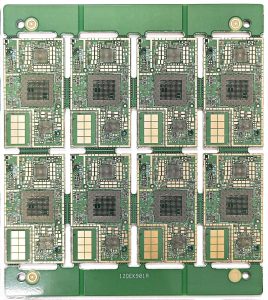
pcb puzzle together
What is PCB Puzzle Together (Panelization)?
PCB panelization is the process of combining multiple individual PCBs into a single panel for more efficient manufacturing, assembly, and handling. The panelized boards are separated into individual PCBs after the assembly process.
Why is PCB Panelization Important?
✔ Improves Manufacturing Efficiency – Reduces machine setup time and increases production speed.
✔ Minimizes PCB Waste – Optimizes material usage to lower costs.
✔ Facilitates Automated Assembly – Enhances pick-and-place efficiency in SMT production.
✔ Prevents PCB Damage – Provides mechanical support during handling and transport.
Types of PCB Panelization Methods
There are several methods to “puzzle together” PCBs into a manufacturing panel, depending on design requirements and assembly techniques.
1. V-Scoring (V-Groove Panelization)
✔ How It Works:
- V-shaped grooves are cut along the PCB surface, allowing easy separation after assembly.
- The board remains partially connected but can be broken apart with minimal force.
✔ Advantages:
- High precision and strength during manufacturing.
- Ideal for rectangular or straight-edged PCBs.
- Compatible with automated depaneling machines.
✔ Best For:
- Rigid PCBs with simple shapes.
- High-volume SMT production.
2. Tab-Route (Breakaway Tab) Panelization
✔ How It Works:
- PCBs are connected by thin breakout tabs with perforated holes.
- The tabs provide mechanical support and are snapped off after assembly.
✔ Advantages:
- Supports irregular-shaped PCBs.
- Reduces mechanical stress on sensitive components.
✔ Best For:
- PCBs with complex shapes.
- Low- to medium-volume production.
3. Solid-Frame Panelization (No Breakaways)
✔ How It Works:
- The PCBs are fully connected within a solid frame.
- Requires routing or laser cutting for separation.
✔ Advantages:
- Provides maximum support and alignment during assembly.
- Reduces stress on fragile PCBs.
✔ Best For:
- Thin PCBs, flex PCBs, and high-precision circuits.
- Boards with BGA, fine-pitch components, or heavy connectors.
4. Mixed Panelization (Combination of V-Scoring and Tab-Route)
✔ How It Works:
- Combines V-scoring and tab-routing for optimal strength and ease of separation.
- Used for complex layouts where different PCBs need different depaneling methods.
✔ Advantages:
- Balances mechanical strength and ease of separation.
- Suitable for boards with different shapes and assembly needs.
✔ Best For:
- High-mix PCB production.
- Applications requiring both rigidity and flexibility.
Key Design Considerations for PCB Panelization
To ensure successful PCB panelization, designers must optimize panel layout, spacing, and routing.
1. PCB Orientation and Layout
✔ Align PCBs in a way that minimizes material waste and improves machine efficiency.
✔ Maintain a consistent panel size (e.g., 250mm x 300mm) for assembly compatibility.
2. Proper Spacing Between PCBs
✔ Leave 2mm – 3mm gaps between PCBs to allow for routing and depaneling.
✔ Avoid placing components too close to panel edges to prevent damage.
3. Tooling Holes and Fiducial Marks
✔ Tooling holes ensure precise alignment during assembly.
✔ Fiducial marks (optical alignment points) help SMT machines accurately place components.
4. Consideration for PCB Warpage and Stress
✔ Thin PCBs (≤0.8mm) require additional support during assembly.
✔ Use crossbars or reinforcement structures to prevent warping.
Best Practices for PCB Panelization
By following industry best practices, engineers can improve yield rates and reduce production costs.
✔ Choose the Right Panelization Method – V-scoring for straight edges, tab-routing for irregular shapes.
✔ Optimize Panel Size – Align with standard PCB fabrication and assembly machines.
✔ Allow Sufficient Spacing – Prevents solder bridging and misalignment.
✔ Use Copper Balancing Techniques – Avoids PCB warping during reflow soldering.
✔ Test Panel Strength Before Mass Production – Ensures easy depaneling without damaging boards.
Challenges in PCB Panelization and How to Overcome Them
Despite its benefits, PCB panelization presents several challenges:
| Challenge | Cause | Solution |
|---|---|---|
| PCB Warping During Soldering | Uneven copper distribution | Use copper balancing techniques |
| Component Damage During Depaneling | Excessive mechanical stress | Optimize depaneling method (V-score or tab-route) |
| High Material Waste | Inefficient panel layout | Improve PCB nesting design |
| Misalignment in SMT Assembly | Lack of fiducials or tooling holes | Add fiducial marks and alignment holes |
Applications of PCB Panelization
PCB panelization is widely used in various high-volume and precision-based industries:
1. Consumer Electronics
✔ Smartphones, tablets, and wearables use panelized PCBs for mass production.
2. Automotive and Industrial Electronics
✔ Engine control units (ECUs), IoT sensors, and automation systems require panelized PCBs for cost-effective assembly.
3. Medical Devices
✔ High-reliability medical PCBs are panelized for efficient manufacturing.
4. Aerospace and Defense
✔ High-layer rigid-flex PCBs are panelized to reduce handling damage and improve quality control.
Conclusion
“PCB puzzle together” or panelization is an essential technique for efficient PCB production, assembly, and cost optimization. Whether using V-scoring, tab-routing, or mixed panelization, manufacturers can enhance productivity, minimize waste, and improve PCB reliability.
By following best design practices, choosing the right panelization method, and addressing potential challenges, Shuoqiang Electronics provides high-quality PCB panelization services for various industries. Contact us today for professional PCB manufacturing solutions! 🚀

- long board pcb
- Flexible PCBs
- Special PCB
- Express Printed Circuit Board
- Pcb Prototype
- LED PCB
- PCB
- Printed Circuit Board
- Pcb meaning
- Pcb manufacturer
- Rigid pcb board
- Rigid Flex PCB
 Quote
Quote
 E-mail