Key Parameters in the PCB Lamination Process In PCB Manufacturing
Introduction
The lamination process is a critical step in PCB (Printed Circuit Board) manufacturing, where multiple layers are bonded together under heat and pressure to form a multilayer PCB. Proper control of key lamination parameters ensures reliable adhesion, dimensional stability, and defect-free boards. The three most important parameters in the lamination process are:
- Heating Rate – Determines resin flow, curing time, and thickness uniformity.
- Pressing Point (Pressure Application Timing) – Balances resin flow and prevents defects like air bubbles and wrinkles.
- Curing Time – Affects material stability, mechanical strength, and overall lamination quality.
Each of these parameters must be carefully optimized to achieve high-quality laminated PCBs while minimizing defects such as resin voids, warpage, copper wrinkles, and delamination.
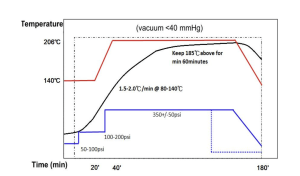
Lamination Process
1. Heating Rate (Temperature Ramp-Up)
Definition
The heating rate refers to the speed at which temperature increases during lamination. It directly influences resin flow, curing reaction, and overall lamination quality.
Effects of Heating Rate on Lamination
| Heating Rate | Advantages | Disadvantages |
|---|---|---|
| Fast Heating Rate | – Shortens total lamination time, increasing efficiency. |
- Increases resin flow, reducing copper wrinkles and voids.
- Helps reduce resin starvation (insufficient adhesive). | – Decreases thickness uniformity, increasing risk of white edges, white corners, and fiber exposure.
- May cause excessive resin flow, leading to delamination.
- Increased risk of thermal stress. | | Slow Heating Rate | – Improves thickness uniformity.
- Reduces thermal stress and risk of delamination.
- Prevents excessive resin flow. | – Increases lamination cycle time.
- Risk of incomplete resin curing.
- Higher chances of copper wrinkles and poor adhesion. |
Optimization Strategy
- The heating rate should be adjusted based on material type, copper thickness, and stack-up design.
- Ideally, temperature should be ramped up quickly to enhance resin flow, but not too fast to cause thickness variations.
- A good practice is to reach the transition point before resin flow peaks, avoiding excessive or insufficient flow.
2. Pressing Point (Pressure Application Timing)
Definition
The pressing point is the moment when full pressure is applied during the lamination cycle. It must be synchronized with the heating rate and resin behavior to avoid defects.
Effects of Pressing Point Timing
| Pressing Point Timing | Effects on PCB Lamination |
| Too Early | – Increased risk of air bubbles trapped inside the PCB. |
- Excessive resin flow leads to thickness non-uniformity.
- More resin escapes, increasing risk of copper wrinkles. | | Too Late | – Resin flow is insufficient, leading to poor bonding and delamination.
- Air pockets remain, creating voids and weak adhesion points.
- Higher chances of copper wrinkles and resin starvation. | | Optimized Pressing Point | – Balanced resin flow prevents resin starvation while ensuring good adhesion.
- Ensures even thickness distribution and reduces defects. |
Optimization Strategy
- The pressing point must be adjusted based on the resin viscosity curve.
- Each PCB layer heats up at a different rate, requiring a balanced pressure application to ensure uniform bonding.
- Typically, pressing should be applied right before the resin flow reaches its peak, ensuring good adhesion without excessive escape.
3. Curing Time
Definition
Curing time refers to the duration for which the PCB stack remains at the final curing temperature, allowing the resin to fully polymerize and solidify.
Effects of Curing Time on Lamination
| Curing Time | Effects |
| Short Curing Time | – Results in incomplete polymerization, leading to dimensional instability. |
- PCBs are more prone to warpage and deformation.
- Higher chances of delamination and weak adhesion. | | Long Curing Time | – Ensures complete resin polymerization, improving mechanical strength.
- Enhances long-term stability and reduces chances of warping.
- Excessively long curing leads to higher production costs, heat wastage, and resin brittleness. |
Optimization Strategy
- Generally, curing should be done at ≥170°C for at least 30 minutes.
- If curing time is too short, the PCB may shrink or warp after production.
- If curing time is too long, resin may become brittle and yellowing may occur.
- Finding the optimal balance based on material properties and PCB design ensures stability without unnecessary energy consumption.
Additional Factors Affecting Lamination
Besides the three main parameters, several other factors can influence lamination quality and process stability:
- Material Properties – Different PCB materials (FR4, high-Tg, Rogers, etc.) require different lamination conditions.
- Copper Thickness – Thicker copper layers retain more heat, affecting the flow and curing of the resin.
- Board Thickness and Layer Count – Thicker boards require longer curing times and optimized heating rates.
- Stack-Up Structure – Symmetric stack-up improves thermal stability and reduces warping.
- Pressure Uniformity – Proper lamination press calibration prevents localized delamination and voids.
Conclusion
The PCB lamination process is a delicate balance of heating rate, pressing point timing, and curing time. By optimizing these parameters, manufacturers can:
- Reduce defects such as air bubbles, copper wrinkles, and resin starvation.
- Improve PCB dimensional stability and reliability.
- Enhance production efficiency while maintaining high-quality standards.
Since different materials, stack-ups, and designs require unique settings, continuous process optimization and real-time monitoring are essential for achieving consistent, defect-free PCBs. Properly adjusting lamination parameters ensures that PCBs meet the demands of high-frequency, HDI, and high-performance applications, supporting the evolving needs of the electronics industry.

- long board pcb
- Flexible PCBs
- Special PCB
- Express Printed Circuit Board
- Pcb Prototype
- LED PCB
- PCB
- Printed Circuit Board
- Pcb meaning
- Pcb manufacturer
- Rigid pcb board
- Rigid Flex PCB
 Quote
Quote
 E-mail