Introduction: Understanding the Importance of PCB Drilling Technologies
Printed circuit boards (PCBs) are the backbone of modern electronic systems, providing mechanical support and precise electrical connections for millions of devices used in consumer electronics, automotive systems, medical instrumentation, and aerospace applications. Among the dozens of steps in PCB manufacturing, drilling is one of the most crucial, since it defines the interconnection pathways between different layers of the board. Without accurate drilling, multilayer PCBs would simply not function.
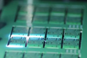
PCB Drilling Technologies have evolved significantly over the past four decades. What was once a slow and purely mechanical process has diversified into multiple drilling approaches that balance speed, cost, and precision. Today, manufacturers primarily rely on three drilling technologies:
-
Mechanical drilling, the traditional method, which uses high-speed rotating drill bits.
-
Laser drilling, which employs advanced CO₂ or UV lasers to create extremely fine microvias.
-
Punching, a cost-effective stamping method used mainly for mass production of simpler PCBs.
The choice of drilling method directly affects not only the production efficiency but also the performance of the PCB itself. Hole precision, wall quality, and aspect ratio all influence electrical conductivity, thermal dissipation, and long-term reliability. Therefore, engineers and designers must carefully consider which drilling technology best suits their design requirements.
In this article, we will conduct a deep technical exploration of these three PCB Drilling Technologies, analyze their advantages and drawbacks, assess their impact on PCB performance, and discuss real-world applications.
PCB Drilling Technologies
Overview of PCB Drilling Technologies
Definition and Role of PCB Drilling Technologies in Manufacturing
In PCB fabrication, drilling is the process of creating vias, through-holes, and mounting holes that serve as electrical interconnections between different copper layers or as mechanical support points for components. The precision of these holes is critical, as they define the conductive pathways that enable signals to travel efficiently and reliably.
PCB Drilling Technologies cover all the methods by which these holes are created. While the basic objective is simple—removing substrate material to form a hole—the complexity arises from the wide range of PCB types. For example:
-
Single-layer PCBs require relatively simple drilling for component leads.
-
Multilayer PCBs involve extremely fine vias with tight tolerances.
-
High-density interconnect (HDI) boards demand microvias smaller than 100 microns, which are only feasible through laser drilling.
Thus, PCB Drilling Technologies not only determine the feasibility of a given PCB design but also constrain or enable innovation in electronics.
Historical Development of PCB Drilling Technologies
The first PCBs in the 1950s and 1960s were relatively simple, and mechanical drilling was sufficient. However, as device complexity grew, new methods had to be developed:
-
1960s–1970s: Mechanical drilling dominated, using tungsten-carbide drill bits.
-
1980s: Miniaturization began driving the need for smaller vias, but mechanical drills struggled with durability and accuracy at tiny diameters.
-
1990s: Laser drilling emerged, particularly with the rise of mobile phones and compact electronics requiring HDI structures.
-
2000s onward: Punching and stamping technologies evolved for high-volume, low-cost consumer electronics, while laser drilling became essential for advanced PCBs.
Today, hybrid manufacturing processes are common, combining mechanical drilling for large through-holes with laser drilling for microvias.
Why PCB Drilling Technologies Are Critical for Precision Electronics
The importance of PCB Drilling Technologies cannot be overstated. A poorly drilled via can lead to:
-
Electrical failures, due to poor copper plating or uneven hole walls.
-
Signal integrity issues, especially in high-frequency PCBs where impedance matching is critical.
-
Reduced mechanical reliability, leading to cracking under thermal or mechanical stress.
On the other hand, optimized drilling technologies can enhance:
-
Thermal dissipation, as precise holes improve copper plating uniformity.
-
Miniaturization, enabling denser interconnections in smartphones, tablets, and IoT devices.
-
Long-term reliability, with vias capable of surviving thousands of thermal cycles.
For example, in aerospace and automotive applications where PCBs are exposed to vibration and extreme temperatures, the durability of drilled vias can determine the overall system lifespan. This makes the selection of PCB Drilling Technologies not just a matter of cost, but of mission-critical reliability.
Mechanical PCB Drilling Technologies
Principles of Mechanical PCB Drilling Technologies
Mechanical drilling is the most traditional and widely used of the PCB Drilling Technologies. It involves the use of a high-speed rotating spindle that drives a tungsten carbide or diamond-coated drill bit into the PCB substrate. The bit physically removes material, creating holes of predetermined diameter and depth.
The mechanics of this process are deceptively simple, but achieving high precision requires advanced control. The drilling machine must ensure:
-
High rotational speed (often 100,000 to 300,000 RPM) to reduce tool deflection and maintain hole roundness.
-
Z-axis accuracy, which determines the exact penetration depth for blind vias.
-
Chip evacuation, since the removed epoxy-glass debris must be cleared to prevent clogging and burning.
Mechanical drilling typically creates through-holes that connect all layers of the PCB. For multilayer boards, these holes are later plated with copper to form conductive vias.
Equipment and Tooling Used in Mechanical PCB Drilling Technologies
Modern PCB factories employ CNC drilling machines capable of handling thousands of holes per panel with micron-level accuracy. Key equipment aspects include:
-
Spindles: Each spindle can drill independently, and high-end machines may have up to 30 spindles operating in parallel.
-
Tool changers: Automatic systems that swap worn drill bits for new ones, ensuring continuous operation.
-
Vacuum extraction: Removes resin dust and glass fibers to maintain hole quality.
-
Registration systems: Optical alignment ensures that drilled holes correspond precisely to copper pad locations.
Drill bits are usually made of tungsten carbide, which balances hardness and toughness. For extremely fine holes (down to 0.1 mm), diamond-coated micro-drills are used to reduce wear.
Advantages and Drawbacks of Mechanical PCB Drilling Technologies
Like all PCB Drilling Technologies, mechanical drilling comes with both strengths and limitations.
Advantages:
-
Versatility: Capable of drilling a wide range of diameters, from large mounting holes to relatively small vias.
-
Mature technology: Well-understood, with abundant equipment suppliers and standardized processes.
-
Cost-effective: For through-holes larger than 0.15 mm, mechanical drilling remains cheaper than laser drilling.
-
High throughput: Multi-spindle machines can handle thousands of holes per minute.
Drawbacks:
-
Tool wear: Drill bits dull quickly, especially when drilling fiberglass-reinforced substrates. Worn tools reduce precision and must be replaced frequently.
-
Minimum hole size limitation: Mechanical drills cannot reliably produce microvias smaller than ~100 microns.
-
Debris and thermal stress: Improper chip evacuation can cause resin smear, reducing plating adhesion.
-
Aspect ratio challenges: Very deep holes with narrow diameters are prone to misregistration and cracking.
In high-frequency applications, poorly drilled mechanical vias can create impedance discontinuities, impacting signal integrity. Therefore, although mechanical drilling is reliable, it must be carefully monitored with strict quality control.
Applications of Mechanical PCB Drilling Technologies in Modern PCBs
Despite its limitations, mechanical drilling is still the backbone of most PCB manufacturing. Applications include:
-
Through-hole PCBs: Widely used in power electronics, automotive systems, and industrial control boards.
-
Multilayer PCBs with plated through-holes (PTH): Essential for connecting all layers in telecommunications and aerospace electronics.
-
Component mounting holes: For connectors, transformers, and power semiconductors requiring large and robust anchor points.
-
Hybrid drilling processes: Many advanced PCBs combine mechanical drilling for large vias and laser drilling for microvias.
For example, in the automotive industry, engine control units (ECUs) often use mechanical drilling for their power and ground vias because of the higher current carrying capacity of larger plated through-holes.
This demonstrates that while mechanical drilling is no longer sufficient for the smallest geometries, it continues to play a vital role in ensuring electrical robustness.
Laser PCB Drilling Technologies
Principles of Laser PCB Drilling Technologies
Laser drilling represents one of the most advanced PCB Drilling Technologies, allowing manufacturers to achieve levels of precision impossible with mechanical methods. Instead of physically cutting material, a focused laser beam delivers concentrated energy that vaporizes the PCB substrate at the target location. The result is a hole with extremely small diameter and excellent shape accuracy.
Two main laser types are used in PCB manufacturing:
-
CO₂ Lasers (Infrared, 9–10 μm wavelength)
-
Well-suited for removing dielectric materials such as FR-4 epoxy.
-
Limited effectiveness when directly drilling copper, as copper reflects infrared light.
-
-
UV Lasers (355 nm wavelength)
-
Capable of ablating both dielectric materials and thin copper foils.
-
Provides finer resolution, making it the preferred choice for microvia formation in HDI boards.
-
The laser drilling process typically involves multiple pulses, each removing a thin layer of material. This minimizes thermal stress, improves edge quality, and ensures precise control over hole depth.
CO₂ vs UV Laser Systems in PCB Drilling Technologies
CO₂ Laser Systems
-
Commonly used for drilling dielectric materials in HDI PCBs.
-
Fast and cost-efficient for creating blind vias in large-scale production.
-
Cannot directly ablate thick copper; usually combined with mechanical drilling or pre-etched openings.
UV Laser Systems
-
Provide significantly higher precision, with hole diameters as small as 20 μm.
-
Effective for cutting both dielectric and thin copper, making them versatile for fine-featured designs.
-
Higher equipment cost compared to CO₂ systems, but essential for advanced consumer electronics like smartphones.
In practice, many PCB manufacturers integrate dual-laser systems, using CO₂ for bulk dielectric removal and UV for final precision shaping. This hybrid approach leverages the speed of CO₂ with the accuracy of UV.
Advantages and Drawbacks of Laser PCB Drilling Technologies
Advantages:
-
Microvia capability: Enables hole diameters below 100 μm, essential for HDI PCBs.
-
Non-contact process: No tool wear, unlike mechanical drilling.
-
Excellent precision: High aspect ratio vias with smooth walls improve plating quality.
-
Flexibility: Can be programmed for complex via patterns without physical retooling.
-
High reliability: Microvias created by laser drilling reduce parasitic inductance, improving high-frequency performance.
Drawbacks:
-
High capital cost: Laser drilling machines are significantly more expensive than mechanical systems.
-
Slower for large holes: Mechanical drilling remains faster for through-holes larger than 0.3 mm.
-
Thermal effects: Improper process control can cause carbonization or damage adjacent copper layers.
-
Energy-intensive: Requires sophisticated cooling and power systems.
Despite these drawbacks, the benefits outweigh the costs for high-end applications, particularly where miniaturization and signal integrity are critical.
High-Density Interconnect (HDI) Applications with Laser PCB Drilling Technologies
HDI PCBs represent the cutting edge of electronic packaging, used in smartphones, tablets, wearables, and advanced computing systems. These boards rely heavily on laser PCB Drilling Technologies to create stacked and staggered microvias that interconnect multiple layers within a very small footprint.
Key benefits in HDI applications include:
-
Space saving: Laser-drilled microvias allow for higher routing density, enabling smaller PCB sizes.
-
Signal integrity: Shorter via stubs reduce reflection and crosstalk in high-speed circuits.
-
Reliability: Laser vias provide better plating uniformity and mechanical stability compared to very fine mechanical vias.
For example, in 5G smartphones, microvias drilled by UV lasers connect fine-pitch components such as RF transceivers and antennas, ensuring high-frequency signals maintain integrity.
Punching PCB Drilling Technologies
Principles of Punching PCB Drilling Technologies
Among the three major PCB Drilling Technologies, punching is often considered the most straightforward and cost-effective method. Instead of removing material with a rotating drill bit or vaporizing it with a laser beam, punching relies on a mechanical stamping process. A sharp die, usually made of hardened tool steel, is pressed into the PCB panel to create a hole or slot in one quick motion.
The process is similar to sheet metal stamping, though adapted for PCB substrates such as FR-4, CEM-1, or flexible polyimide films. Punching is especially useful for non-plated holes, tooling holes, and repetitive geometries in low-complexity boards. Once the die is fabricated, the same shape can be reproduced thousands or even millions of times with extremely high throughput.
Punching technology is most often applied to single-layer or double-layer PCBs where vias are not as critical to high-frequency or fine-pitch performance. For complex multilayer or HDI boards, punching is rarely used, as it lacks the precision and adaptability required.
When Punching PCB Drilling Technologies Are Cost-Effective
The greatest strength of punching lies in its economies of scale. While designing and fabricating a precision punching die can be expensive upfront, the per-hole cost drops dramatically once high-volume production begins.
Punching is cost-effective in scenarios such as:
-
Consumer electronics with simple PCBs – calculators, toys, or low-cost home appliances.
-
Mass-market LED lighting modules – where holes are needed for mechanical mounting and heat dissipation, but not for high-density routing.
-
Flexible PCBs – punching is frequently used in FPC production, where polyimide sheets can be stamped cleanly with minimal thermal or mechanical stress.
-
Tooling holes – alignment and registration holes in PCBs, which must be repeated accurately across thousands of boards.
In these contexts, punching can produce hundreds of holes per second, far outpacing both mechanical and laser drilling in terms of speed.
Advantages and Drawbacks of Punching PCB Drilling Technologies
Advantages:
-
Ultra-high speed: Entire arrays of holes can be created in a single press stroke.
-
Low per-unit cost in mass production: Once the die is made, production costs become negligible compared to drilling.
-
Consistency: Every punched hole is nearly identical in size and shape, provided the die is well-maintained.
-
Suitability for flexible substrates: Punching can process thin films without thermal damage, unlike lasers.
Drawbacks:
-
High upfront cost: Fabricating precision dies is expensive, making punching unsuitable for low-volume or prototype production.
-
Limited precision: Hole sizes and tolerances are less accurate than those from laser or mechanical drilling.
-
Design inflexibility: Once the die is fabricated, modifying hole patterns is costly and time-consuming.
-
Not viable for microvias or HDI: Punching cannot achieve the fine geometries required for advanced electronics.
In short, punching is ideal for cost-driven, high-volume, low-complexity PCBs, but not for advanced electronics requiring miniaturization or high-frequency signal integrity.
Mass Production Use Cases for Punching PCB Drilling Technologies
Punching technology continues to play a role in several industries:
-
Household appliances – PCBs in washing machines, microwaves, and refrigerators often use punched tooling holes.
-
Automotive lighting – LED driver boards for headlights and taillights are sometimes punched for thermal via arrays.
-
Flexible circuit boards – punching enables fast, clean cutting of flexible circuits used in printers, cameras, and consumer gadgets.
-
Disposable medical devices – low-cost medical PCBs, such as test strip readers, may use punched holes to minimize production costs.
A typical example is in low-cost LED modules, where manufacturers need to produce millions of identical boards. Using punching, they can cut production time drastically while maintaining acceptable tolerances.
Comparative Analysis of PCB Drilling Technologies
Speed and Precision Comparison among the Three PCB Drilling Technologies
When comparing the speed and precision of the three main PCB Drilling Technologies, clear distinctions emerge:
-
Mechanical Drilling:
-
Speed: High, especially with multi-spindle CNC drilling machines. A single machine can drill tens of thousands of holes per hour.
-
Precision: Moderate, limited by tool wear and drill bit deflection. Reliable for hole diameters above ~0.15 mm.
-
Suitability: Excellent for general through-holes but challenged by microvia requirements.
-
-
Laser Drilling:
-
Speed: Lower than mechanical drilling for large holes but extremely fast for microvias (<100 μm).
-
Precision: Superior, capable of producing hole diameters as small as 20 μm with high consistency.
-
Suitability: Essential for HDI PCBs, where precision and micro-scale interconnections are critical.
-
-
Punching:
-
Speed: By far the fastest. Hundreds of holes can be produced in a single press stroke.
-
Precision: Lowest among the three, with tolerances typically acceptable only for non-critical holes.
-
Suitability: Excellent for high-volume, low-cost production but not for advanced electronics.
-
From this comparison, it becomes evident that laser drilling dominates in precision, punching dominates in speed, while mechanical drilling offers a balanced middle ground for versatility.
Cost Considerations of PCB Drilling Technologies
Cost is often the deciding factor in choosing drilling technologies.
-
Mechanical Drilling:
-
Equipment cost: Moderate. CNC machines are widely available.
-
Operating cost: Relatively low, though frequent bit replacement adds to maintenance expenses.
-
Per-hole cost: Efficient for medium to large holes, but costs rise when very small holes are needed.
-
-
Laser Drilling:
-
Equipment cost: High. UV laser systems are expensive to purchase and maintain.
-
Operating cost: Moderate to high due to power consumption and cooling requirements.
-
Per-hole cost: Very efficient for microvias, but not cost-effective for large holes.
-
-
Punching:
-
Equipment cost: Low to moderate. Press machines are simple, but custom dies are expensive.
-
Operating cost: Very low once dies are fabricated.
-
Per-hole cost: Negligible in mass production, making it the most economical option for large-scale manufacturing.
-
In summary, punching is cheapest for high-volume production, mechanical drilling is cost-effective for versatile requirements, and laser drilling is the most expensive but unavoidable for advanced PCBs.
Reliability and Durability of Vias Produced by Different PCB Drilling Technologies
The long-term reliability of vias is one of the most important metrics when selecting PCB Drilling Technologies.
-
Mechanical Drilling:
-
Produces robust through-holes suitable for power and ground connections.
-
Risks: Smear on hole walls may reduce copper adhesion if not cleaned properly.
-
Durability: Good for larger vias, but less effective for very small geometries.
-
-
Laser Drilling:
-
Produces microvias with smooth walls, excellent for copper plating.
-
Risks: Poor process control may cause carbonization or incomplete ablation.
-
Durability: High, especially in HDI PCBs where microvias undergo fewer thermal cycles.
-
-
Punching:
-
Produces holes with rougher edges, acceptable for mechanical or non-critical applications.
-
Risks: Deformation of hole shape if the die wears out.
-
Durability: Adequate for low-stress applications but unsuitable for high-frequency or mission-critical PCBs.
-
Thus, for applications where long-term reliability is essential (aerospace, medical devices, automotive safety systems), laser and mechanical drilling outperform punching.
Impact on High-Frequency Signal Performance
The choice of PCB Drilling Technologies also affects high-frequency and high-speed electronic performance:
-
Mechanical Drilling: Vias tend to be deeper and wider, creating longer stubs. These stubs introduce unwanted capacitance and inductance, degrading signal integrity in high-speed circuits. Careful back-drilling is sometimes required to remove stubs.
-
Laser Drilling: Microvias produced by lasers minimize stub length, reduce parasitic effects, and improve impedance control. This makes laser drilling the best choice for RF PCBs, 5G devices, and high-speed computing boards.
-
Punching: Rarely used in high-frequency designs because of low precision and rough edges, which introduce variability and potential reflections.
In practice, designers of high-frequency PCBs almost always specify laser drilling for microvias to ensure signal quality.
Advantages of PCB Drilling Technologies and Their Impact on PCB Performance
Electrical Performance Advantages of PCB Drilling Technologies
The selection of PCB Drilling Technologies has a direct impact on the electrical performance of a circuit board, especially in high-frequency and high-speed designs.
-
Mechanical Drilling:
-
Provides reliable plated through-holes for power and ground distribution.
-
Larger hole diameters lead to longer stubs, which can degrade high-frequency performance due to parasitic capacitance and inductance.
-
Back-drilling can mitigate stub effects, but this increases processing cost.
-
-
Laser Drilling:
-
Enables creation of microvias with extremely short stubs.
-
Reduces signal distortion and reflections, improving impedance control.
-
Essential for RF applications such as 5G antennas, satellite communications, and high-speed data transmission.
-
-
Punching:
-
Holes produced are acceptable for mechanical stability but generally unsuitable for high-frequency signal routing.
-
Variability in hole geometry can affect impedance uniformity, reducing overall electrical performance.
-
In modern designs, laser drilling clearly outperforms in terms of electrical advantages, as it directly supports high-speed signal integrity.
Thermal Management and Heat Dissipation
Heat dissipation is another critical factor in PCB design, and PCB Drilling Technologies contribute in different ways:
-
Mechanical Drilling:
-
Can produce large arrays of thermal vias, effectively transferring heat from components (e.g., power transistors) to copper planes or heat sinks.
-
Reliable for boards handling significant power loads.
-
-
Laser Drilling:
-
Supports dense microvia arrays for localized heat spreading in compact devices.
-
Common in smartphones and tablets, where thermal constraints are severe due to miniaturization.
-
-
Punching:
-
Often used to create ventilation or mounting holes in LED driver boards, indirectly aiding heat dissipation.
-
Less effective in controlled thermal pathways compared to drilled vias.
-
In practice, a hybrid approach is often used: mechanical drilling for large thermal vias, laser drilling for microvia heat spreading, and punching for high-volume, cost-driven designs.
Structural Reliability and Mechanical Stability
The long-term mechanical stability of PCBs is heavily influenced by drilling methods:
-
Mechanical Drilling:
-
Well-established for producing robust through-holes that endure multiple thermal cycles and mechanical stresses.
-
Potential issue: hole wall roughness or smear may reduce plating adhesion if not properly cleaned.
-
-
Laser Drilling:
-
Produces clean, smooth holes, ensuring excellent copper plating adhesion.
-
Microvias tend to have higher reliability when properly processed, but they can suffer from via-in-pad failures if subjected to extreme thermal cycling.
-
-
Punching:
-
Offers less structural precision, and holes may suffer from edge deformation over time.
-
Adequate for consumer-grade, short-lifespan products but not for mission-critical electronics.
-
From an engineering perspective, laser and mechanical drilling dominate in reliability, while punching is acceptable only for low-cost products where longevity is not paramount.
Miniaturization and Design Flexibility
One of the most significant advantages of modern PCB Drilling Technologies is enabling the ongoing trend toward miniaturization:
-
Mechanical Drilling:
-
Limited by drill bit diameters, making it less suitable for ultra-compact designs.
-
Still valuable for power connectors and mechanical strength requirements.
-
-
Laser Drilling:
-
Enables extremely fine microvia structures (down to 20 μm), critical for High-Density Interconnect (HDI) boards.
-
Facilitates 3D stacking of vias, allowing designers to fit more functionality into smaller footprints.
-
Supports cutting-edge applications such as foldable smartphones, medical implants, and aerospace miniaturization.
-
-
Punching:
-
Offers very little design flexibility since once a die is made, modifications are costly.
-
Best suited for standardized products where design iteration is minimal.
-
In essence, laser drilling is the cornerstone of modern miniaturization, while mechanical drilling complements it in traditional roles, and punching supports mass-market cost efficiency.
Author’s Insight on Performance Impact
From my perspective, the biggest transformative effect of drilling technology lies in how it allows engineers to push the boundaries of performance and size simultaneously. Without microvia drilling by lasers, today’s smartphones would either be much bulkier or significantly less powerful. Similarly, without mechanical drilling, we would not have the robust power distribution networks needed in high-power electronics.
Punching, though often overlooked, plays a critical role in democratizing electronics by keeping costs low, ensuring that devices like LED lamps and household appliances remain affordable to the masses.
Thus, the true impact of PCB Drilling Technologies is holistic: they simultaneously enable performance, reliability, miniaturization, and cost control—each serving different segments of the electronics industry.
Choosing the Right PCB Drilling Technologies for Your Project
Selecting the right PCB Drilling Technologies is not simply a matter of cost—it is a strategic design decision that influences the reliability, performance, and manufacturability of the final product.
Key Decision Factors for PCB Drilling Technologies
-
Cost Considerations
-
Mechanical drilling: Cost-effective for through-holes and medium-density boards.
-
Laser drilling: Higher equipment cost, but necessary for HDI and microvias.
-
Punching: Lowest per-hole cost, but limited in precision and flexibility.
-
-
Production Volume
-
High-volume, simple boards → Punching is unbeatable.
-
Low-to-medium volume, complex boards → Mechanical drilling remains optimal.
-
High-volume, high-density advanced designs → Laser drilling is indispensable.
-
-
Precision and Miniaturization
-
For HDI designs, 5G boards, wearables, and medical implants, laser is the only viable option.
-
Mechanical drilling cannot reliably achieve via diameters below ~0.2 mm.
-
-
Reliability and Environmental Conditions
-
Automotive, aerospace, industrial → Mechanical drilling ensures structural stability.
-
Consumer and telecom electronics → Laser drilling ensures electrical performance.
-
Recommended Scenarios for Each Drilling Method
-
Mechanical PCB Drilling Technologies:
-
Best for thicker, multi-layer PCBs with high current capacity.
-
Power electronics, automotive ECUs, and industrial systems.
-
-
Laser PCB Drilling Technologies:
-
Best for HDI, microvias, high-frequency circuits.
-
Smartphones, wearables, radar, aerospace, and medical implants.
-
-
Punching PCB Drilling Technologies:
-
Best for simple, repetitive, large-scale boards.
-
LED lighting, consumer appliances, budget electronics.
-
Balancing Performance with Manufacturing Constraints
When choosing a drilling method, engineers must balance:
-
Signal integrity requirements (favor laser).
-
Mechanical strength and reliability (favor mechanical).
-
Cost and scalability (favor punching).
In many modern PCB projects, a hybrid approach is the true solution. For example:
-
Mechanical for through-holes.
-
Laser for HDI microvias.
-
Punching for secondary, repetitive features.
Conclusion – The Strategic Role of PCB Drilling Technologies
Throughout this article, we have explored PCB Drilling Technologies—mechanical drilling, laser drilling, and punching—from their principles to their practical applications, advantages, limitations, and long-term implications for the electronics industry.
Key Takeaways
-
Mechanical PCB Drilling Technologies
-
The backbone of traditional PCB manufacturing.
-
Excels in through-holes, reliability, and large-current designs.
-
Essential for automotive, industrial, and power electronics.
-
-
Laser PCB Drilling Technologies
-
The enabler of miniaturization and HDI.
-
Allows via diameters below 100 µm, critical for smartphones, 5G boards, aerospace, and medical devices.
-
Femtosecond lasers will continue pushing the boundaries of precision.
-
-
Punching PCB Drilling Technologies
-
The most cost-efficient solution for mass production.
-
Best suited for LED lighting, consumer appliances, and cost-driven designs.
-
Limited in precision but unbeatable in throughput.
-
Strategic Role in PCB Performance
Drilling is not a background process—it is a performance-defining step in PCB manufacturing. The size, smoothness, and integrity of vias directly affect:
-
Signal integrity in high-speed circuits.
-
Thermal performance in power electronics.
-
Reliability under thermal cycling and mechanical stress.
A poorly chosen or poorly executed drilling method can undermine even the best PCB design. Conversely, the right drilling technology elevates product performance and lifespan.
The Future of PCB Drilling Technologies
Looking forward, the industry will increasingly embrace:
-
Hybrid workflows, combining mechanical for robustness, laser for microvias, and punching for cost efficiency.
-
AI-driven optimization, where machine learning monitors drilling quality in real time.
-
Sustainability, with greener desmear and recycling methods to reduce environmental impact.
-
Global supply chain resilience, with manufacturers diversifying suppliers and ensuring compliance with IPC, ISO, and UL standards.
FAQs on PCB Drilling Technologies
1. What is the difference between rolled copper foil and electrolytic copper foil?
-
Rolled copper foil: Produced by mechanically rolling copper into thin sheets. It offers excellent surface quality, ductility, and mechanical strength, making it ideal for flexible PCBs.
-
Electrolytic copper foil: Produced by electro-deposition. It is more cost-effective and widely used in rigid PCBs, with slightly lower mechanical performance but good overall conductivity.
2. How does laser drilling differ from mechanical drilling in PCB Drilling Technologies?
-
Mechanical drilling:
-
Uses carbide drill bits.
-
Ideal for through-holes and thicker boards.
-
Limited to diameters above ~0.15–0.20 mm.
-
-
Laser drilling:
-
Uses UV or femtosecond lasers.
-
Ideal for microvias (<100 µm) in HDI designs.
-
Produces cleaner, smaller holes with minimal stress.
-
3. What factors affect via reliability in PCB Drilling Technologies?
-
Drill Wall Smoothness: Rough walls reduce plating adhesion, leading to cracks.
-
Aspect Ratio: High aspect ratio (depth vs. diameter) can stress plating layers.
-
Thermal Cycling: Repeated expansion and contraction can cause micro-cracks.
-
Cleaning Processes: Incomplete desmear leads to poor plating conductivity.
4. Why is punching still relevant in PCB Drilling Technologies when laser and mechanical methods seem superior?
Punching offers:
-
Extremely low cost per hole in mass production.
-
High throughput—thousands of identical holes can be produced rapidly.
-
Minimal tool wear cost compared to mechanical bits.
However, its limitations—lack of precision, tool shape restrictions—mean it’s suitable mainly for LED lighting, appliance boards, and cost-driven electronics, not for high-density PCBs.
5. How do PCB Drilling Technologies affect overall PCB performance?
-
Signal Integrity: Smaller, cleaner laser-drilled vias reduce parasitic capacitance/inductance.
-
Thermal Management: Mechanical vias with thick copper improve heat dissipation.
-
Reliability: Well-drilled vias prevent cracks and delamination under stress.
-
Cost and Scalability: Punching lowers costs in repetitive designs, while hybrid methods balance price and performance.

- long board pcb
- Flexible PCBs
- Special PCB
- Express Printed Circuit Board
- Pcb Prototype
- LED PCB
- PCB
- Printed Circuit Board
- Pcb meaning
- Pcb manufacturer
- Rigid pcb board
- Rigid Flex PCB
 Quote
Quote
 E-mail