Exploring the PCB Definition:
A printed circuit board (PCB) is a flat board that connects and supports electronic components using etched copper pathways. It forms the foundation of nearly all electronic devices. This article is produced by engineering experts from SQPCB, a professional PCB manufacturer with over 12 years of experience serving global OEMs and electronics developers.
When was the last time you stopped to think about the unsung heroes of the devices that power your life? You might gaze at your smartphone, tablet, or even your car’s dashboard and appreciate the sleek design, the user-friendly interface, and the seamless performance. But have you ever considered the intricate network of connections that make all of this possible? That network is not just a collection of wires or chips—it’s the Printed Circuit Board (PCB).

What are printed circuit boards
If you’ve never heard of a PCB, or if you’ve heard the term tossed around without really knowing what it means, now’s the time to change that. PCB definition plays a crucial role in understanding the heart of modern electronics. PCBs are the backbone of virtually every modern electronic device, from the simplest remote control to the most complex medical equipment. Yet, despite their critical importance, most people remain oblivious to their role.
What is pcb mean, Why should you care about PCB boards? Because without them, your smartphone wouldn’t fit in your pocket, your laptop wouldn’t open up to a crisp display, and your car wouldn’t even start. The PCB board definition is simple: it is the foundation that connects and powers all the components within your device, keeping everything running smoothly and efficiently. But what exactly are PCBs, how do they work, and why do they matter so much in today’s fast-paced, technology-driven world?
Let’s dive into the world of PCBs, unraveling the mystery behind their definition, their function, and their undeniable importance in shaping the future of electronics.

Exploring the PCB Definition
PCB Definition, What Exactly is a PCB?
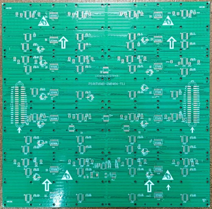
A Printed Circuit Board (PCB) is, at its core, an electrical pathway that physically supports and connects the electronic components within a device. Imagine a puzzle, where each piece represents an electrical component—like a resistor, capacitor, or microchip. The PCB board is the intricate map that not only holds all of those pieces together but also ensures they communicate with one another effectively. It is the bridge that allows the various parts of an electronic system to function as a cohesive whole.
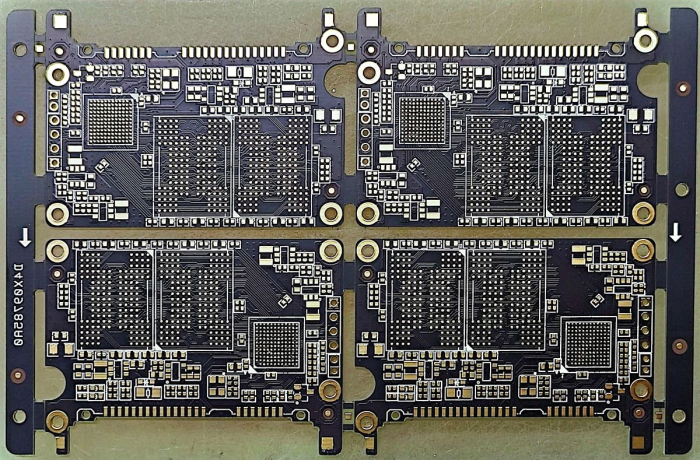
In more technical terms, a PCB is a flat, rigid (or sometimes flexible) board made from non-conductive material, usually fiberglass or composite epoxy. It is covered with a conductive layer—often copper—that is etched into intricate patterns that form electrical traces, connecting different components. The traces are thin lines of copper that carry electrical signals between various parts of the circuit. Pads are the spots where components are mounted, and vias are tiny holes drilled through the board to connect traces from different layers.
To put it simply, PCBs are the lifeblood of any electronic device, enabling the flow of electricity and ensuring that each component works in harmony. The PCB board parts and definition are fundamental for understanding how devices operate. every PCB supplier must know this importance
PCB Definition, How Do PCBs Work?
Now that we’ve explored the definition of a PCB, let’s zoom in on how these boards function. At the most basic level, PCBs serve as the platform on which electrical components can be placed and connected. But the magic truly happens in the detailed engineering that goes into designing and manufacturing these boards. A PCB’s role is not just to support the physical components; it also dictates the way electrical signals are transmitted between them, ensuring that the entire device operates with precision.
The Electrical Pathways:
The most obvious function of a PCB board is to carry electrical signals between components. These signals travel through copper traces, which are carefully designed to optimize the flow of electricity. In fact, the width, shape, and placement of these traces can significantly impact the performance of the entire system. Poorly designed traces can cause unwanted noise, signal distortion, or even complete circuit failure.
The Power Supply:
The PCB board also plays a pivotal role in distributing power across the device. From the battery or power source, the PCB ensures that the right amount of voltage reaches each component. Think of it as a highway system, where the power supply is the starting point, and the individual components are the exits. The PCB board helps navigate the power along these routes to make sure everything functions smoothly.
Signal Integrity:
In today’s world, the demand for high-speed, high-frequency electronics has reached unprecedented levels. The PCB board is at the forefront of this challenge, requiring careful design to maintain signal integrity—the quality of the electrical signals traveling through the traces. Poor signal integrity can lead to delays, data loss, and malfunctions. Engineers often use advanced techniques such as impedance matching, controlled trace widths, and ground planes to reduce interference and ensure signals remain clean and stable.
Thermal Management:
Electronics generate heat, and that heat needs to be dissipated to prevent components from overheating and failing. Certain PCBs, like aluminum PCBs, are specifically designed to improve heat dissipation. These PCBs are used in high-power applications, such as LED lighting or power supply circuits, where heat management is critical.
The Full Manufacturing Process of a PCB
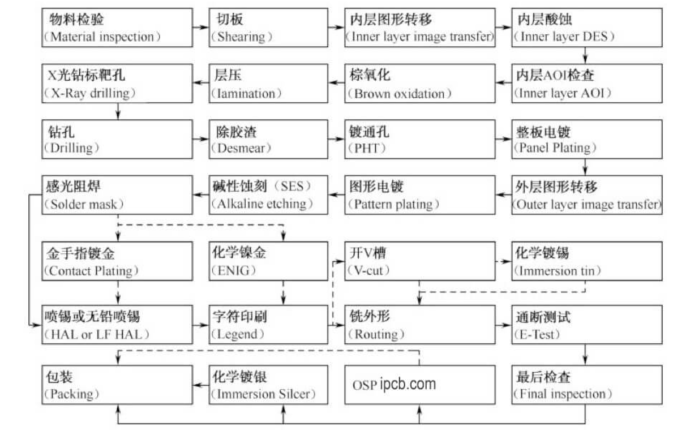
Ready for a deep dive? Here’s how a bare board comes to life—step by step. From fiberglass sheet to functional circuit, this process is where precision meets technology:

whats pcb manufacturing process
1. PCB Boards Manufacturing: Cutting the Raw Material
The manufacturing process begins with cutting the raw PCB material. The material, typically fiberglass-reinforced copper foil, is cut to the required size. The accuracy of cutting is critical, with a tolerance of +/-2mm. Common material sheet sizes include 36”*48”, 40”*48”, and 42”*48”. Material utilization is important for reducing waste, and in special cases, materials can be mixed for cutting to optimize production efficiency.
2. PCB Boards Manufacturing: Inner Layer Processing
This stage involves several sub-processes:
Pre-treatment: Cleaning and preparing the laminate to ensure a contaminant-free surface.
Coating: Applying a photosensitive coating on the laminate surface.
Exposure: Using a photomask to expose the coating to UV light, transferring the design pattern onto the laminate.
Development and Etching: Developing the exposed pattern and removing unwanted copper using a chemical etching solution.
Drilling: Drilling holes for vias and component leads.
AOI (Automated Optical Inspection): Conducting visual inspection to ensure quality.
At SQPCB, advanced techniques such as LDI (Laser Direct Imaging) exposure machines and fully automated coating and baking lines are used. The use of LDI technology minimizes film shrinkage issues, ensuring precise alignment and reducing registration errors. This innovation helps maintain controlled shrinkage within 0.1um, improving the overall quality of the inner layers.
3. Lamination and Pressing
The lamination process involves the bonding of multiple layers to create multi-layer PCBs. This step includes:
Brown-Out and Riveting: Pre-pressing the laminate to form a stable base.
Pre-Stacking: Aligning the stacked layers of copper, laminate, and prepregs.
Pressing: Applying heat and pressure to bond the layers together.
X-ray Drilling Targets: Drilling targets are aligned and inspected using X-ray systems.
Edge Trimming and Grinding: Trimming the edges and ensuring uniformity in thickness.
Pressing is one of the most critical steps in multi-layer PCB production. SQPCB has optimized this process by selecting structures that not only meet the required board thickness but also improve impedance control. Materials such as 7628 are selected over more expensive options like 2116, significantly reducing costs while ensuring high performance.
4. Drilling Process
Drilling is a crucial step for creating holes for vias and through-hole components. It involves:
Pre-Drilling: Initial drilling to prepare the material for deeper cuts.
Drill Bit Grinding: Ensuring the drill bits are sharpened to maintain precision.
Pinning and Drilling: Ensuring accurate hole placement and depth.
Drill Bit Retirement and Peak Polishing: Polishing drill bits after 3,000-5,000 holes to maintain their effectiveness.
SQPCB uses linear motor-driven drilling machines, ensuring high-speed and high-precision drilling. These machines guarantee hole accuracy and consistency, ensuring that all holes meet IPC standards with a tolerance of +/-2mil.
5. Electroplating Process
Electroplating is essential for copper deposition inside drilled holes and on the PCB surface. The process includes:
High-pressure Water Washing: Ensuring the board is clean before electroplating.
PTH (Plated Through-Hole): Plating copper inside the holes for electrical conductivity.
Copper Electroplating: Depositing a thin layer of copper onto the surface and inside the holes to ensure good electrical connections.
SQPCB uses renowned electroplating equipment, investing in high-quality systems that improve yield and reduce the failure rate. While equipment costs may be higher, the long-term benefits of reduced downtime and superior quality outweigh the initial investment.
6. Outer Layer Processing
After the inner layers are completed, the outer layer processing begins. It includes:
Pre-treatment: Cleaning the copper surface before applying the protective coatings.
Film Lamination: Applying a protective film for further processing.
Exposure and Development: Using LDI technology to transfer the design onto the outer layer.
Etching and Removal: Removing the unwanted copper, leaving behind the designed circuit pattern.
AOI and Impedance Testing: Ensuring the design meets the required impedance and quality standards.
At SQPCB, LDI exposure machines with linear motor and optical scale control help achieve shrinkage accuracy within 0.1um, ensuring excellent alignment and reducing defects caused by manual handling.
7. Solder Mask Application
A solder mask is applied to the PCB to protect copper traces and prevent solder bridges during the assembly process. The steps include:
Pre-treatment and Silk Printing: Printing the solder mask onto the PCB.
Pre-baking: Pre-curing the solder mask to harden it before exposure.
Exposure and Development: Using UV light to expose and harden the mask where needed.
SQPCB implements automated solder mask applications, significantly reducing manual errors such as solder mask shift or incorrect pad coverage. This system helps maintain uniformity and ensures a high-quality finish for all PCBs.
8. Text and Legend Printing
Text and legends are applied to the PCB to mark components, references, and other essential information. The process includes:
Silk Screen and Inkjet Printing: Printing labels and other markings.
Post-Baking: Curing the printed ink to ensure durability.
SQPCB uses linear motor-driven inkjet printing machines, achieving exceptional control over shrinkage and print accuracy. This technology reduces defects caused by misalignment and guarantees clear, legible text.
9. Surface Finishing
A surface finish is applied to exposed copper areas to protect against oxidation and improve solderability. This step includes:
Gold Immersion (ENIG), HASL, or OSP: The choice of surface finish is based on customer requirements for durability and solderability.
10. Final Inspection and Electrical Testing
Before assembly, PCBs undergo a series of tests to ensure their functionality:
Electrical Testing: Detects open circuits, short circuits, or misalignments.
Flying Probe Testing and AOI: Ensure the PCB meets design specifications.
Final inspection is essential to ensure that no defects are present and the PCBs meet industry standards before packaging.
Why Do PCBs Matter?
PCBs are indispensable to modern electronics. They act as the foundation upon which everything else is built. But why should you really care about them? Let’s explore some of the top reasons why PCBs matter:
Enabling Innovation:
PCBs are at the heart of every technological advancement. From the smartphone in your pocket to the complex machinery used in medical devices, PCBs make it all possible. They are the silent enabler, providing the infrastructure for more efficient, faster, and smaller devices. Without PCBs, there would be no smartphones, laptops, smart cars, or even many of the life-saving medical technologies we rely on.
Miniaturization of Electronics:
One of the most impressive feats in electronics is how manufacturers have managed to pack more power into smaller, more portable devices. Thanks to the flexibility and versatility of PCBs, it is possible to create high-performance circuits within increasingly compact spaces. The ever-shrinking size of devices is a direct result of innovations in PCB design and manufacturing.
Cost Efficiency:
Without PCBs, electronic devices would be far more costly to produce. PCBs offer a streamlined, efficient way to interconnect and support electronic components at scale. The design and manufacturing of PCBs are now so advanced that they can be produced with precision and speed, making mass production of high-quality electronics feasible at competitive prices.
Reliability:
As electronics become more integral to our daily lives, reliability is key. The design of a PCB is crucial to ensuring that devices perform reliably over time. Engineers carefully consider factors such as durability, power handling, and resistance to environmental factors like moisture and temperature. A well-designed PCB will ensure that your device remains operational, even in challenging conditions.
Safety:
Many industries, from aerospace to medical devices, rely on safety-critical systems. In these environments, PCB design is not just about functionality—it’s about ensuring the system works under pressure and without failure. Safety certifications, like UL and ISO, ensure that PCBs meet the rigorous standards necessary for these applications.
Conclusion: Why PCBs Are More Important Than Ever
Printed Circuit Boards aren’t just components—they’re the framework on which digital innovation is built.
From powering the device in your pocket to controlling industrial systems, PCBs play a critical role in shaping modern life. As demands grow, the need for reliable, custom printed circuit board solutions grows too.
That’s where SQPCB shines—supporting your ideas from concept to completion with professional-grade PCB services.
FAQs About Printed Circuit Boards
Q1: What’s the difference between a PCB and a motherboard?
A: A PCB (Printed Circuit Board) is a general term for any board that mechanically supports and electrically connects electronic components using conductive pathways. A motherboard is a specific type of PCB—typically the main board in a computer system—that houses key components like the CPU, RAM, chipset, and expansion slots. While all motherboards are PCBs, not all PCBs serve as motherboards. PCBs can be found in everything from USB drives and remote controls to medical instruments and industrial machines.
Q2: How long does PCB prototyping take?
A: The turnaround time for PCB prototyping depends on the complexity, layer count, and manufacturing capabilities. Standard prototypes typically take 5–7 working days, while express PCB services—such as those offered by SQPCB—can deliver within 24 to 72 hours. Rapid prototyping is essential during the R&D phase, enabling fast iteration, real-time testing, and quicker time-to-market. This speed is particularly valuable for startups, product validation, and pilot production runs.
Q3: What’s the typical cost of a PCB?
A: PCB pricing is influenced by several factors: board size, layer count, material type, copper thickness, surface finish, hole count, and order volume. For example, a simple 2-layer FR4 board (100mm x 100mm) might cost $14–$30 per piece at low volumes, while a 10-layer HDI board with ENIG finish could exceed $300–$400 per sample. Prototyping services like EASY PCB offer cost-effective options for early-stage development, while larger batches benefit from economies of scale.
Q4: Can PCBs be recycled?
A: Yes, but the process is complex and depends on the material composition. PCBs with gold-plated contacts or valuable components (e.g., from telecom or server boards) can be recycled for precious metals, while boards made from RoHS-compliant, eco-friendly materials are easier to process with lower environmental impact. Mechanical separation, chemical stripping, and pyrolysis are common recycling methods, though not all PCBs are economically viable to recycle at small scale.
Q5: What materials are used in high-frequency PCBs?
A: For RF or microwave applications (above 500 MHz), standard FR4 is often insufficient due to high dielectric losses. Instead, manufacturers use low-loss dielectric substrates like:
Rogers 4350B, Rogers 4450F, 5880: Industry-standard for low Dk and low loss tangent.
PTFE (Teflon-based): Excellent for high-frequency transmission but requires advanced processing.
Ceramic-filled composites: Offer high thermal stability and excellent RF performance.
These materials are commonly used in 5G infrastructure, radar systems, aerospace, and automotive ADAS modules where signal integrity and impedance control are critical.
- long board pcb
- Flexible PCBs
- Special PCB
- Express Printed Circuit Board
- Pcb Prototype
- LED PCB
- PCB
- Printed Circuit Board
- Pcb meaning
- Pcb manufacturer
- Rigid pcb board
- Rigid Flex PCB

 Quote
Quote
 E-mail