Introduction to Panel Plating in PCB Manufacturing
1.1 Understanding Panel Plating
Panel plating is a fundamental process in printed circuit board (PCB) manufacturing, involving the uniform deposition of a conductive material, typically copper, across the entire surface of a PCB panel. This technique ensures consistent electrical connectivity and prepares the board for subsequent circuit patterning and component assembly. By covering the entire panel, including through-holes and surface pads, panel plating establishes a solid foundation for the PCB’s electrical pathways.
1.2 Importance of Panel Plating in PCB Production
The significance of panel plating in PCB production cannot be overstated. It serves as the initial step in creating reliable interconnections within the board, directly impacting the PCB’s performance, durability, and compliance with design specifications. A well-executed panel plating process ensures uniform copper thickness, which is crucial for maintaining consistent impedance and enhancing the mechanical strength of the board.
1.3 Overview of the Panel Plating Process
The panel plating process involves several key stages:
-
Surface Preparation: Cleaning the PCB panel to remove contaminants and oxides, ensuring optimal adhesion of the plating material.
-
Electrolytic Copper Deposition: Immersing the panel in an electrolytic bath where copper ions are deposited onto the surface and through-holes, forming a uniform conductive layer.
-
Post-Plating Treatments: Applying additional coatings or treatments to protect the copper layer and prepare the panel for subsequent manufacturing steps.
Each stage must be meticulously controlled to achieve the desired electrical and mechanical properties in the final PCB.
Panel plating
2. Panel Plating Techniques and Methodologies
2.1 Traditional Panel Plating Methods
Traditional panel plating methods involve immersing the entire PCB panel into a plating bath, allowing for the deposition of a uniform copper layer across all surfaces. This approach is straightforward and effective for standard PCB designs where uniform copper thickness is required.
2.2 Advanced Panel-Plating Technologies
With the evolution of PCB designs, advanced panel plating technologies have been developed to address more complex requirements. Techniques such as pulse plating and reverse pulse plating offer improved control over deposit characteristics, enabling the production of high-density interconnects and fine-line circuitry.
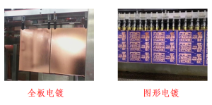
2.3 Comparison Between Panel-Plating and Pattern Plating
Panel plating and pattern-plating are two distinct methodologies in PCB manufacturing:
-
Panel Plating: Involves plating the entire panel uniformly before the circuit pattern is defined.
-
Pattern Plating: Involves plating only the areas defined by the circuit pattern, using a photoresist to mask off unwanted regions.
The choice between these methods depends on factors such as design complexity, required precision, and manufacturing capabilities.
3. Materials Used in Panel-Plating
3.1 Conductive Materials for Panel-Plating
Copper is the primary conductive material used in panel-plating due to its excellent electrical conductivity and reliability. In some applications, additional metals like nickel or gold may be used for specific performance characteristics.
3.2 Chemical Solutions and Electrolytes
The plating process utilizes chemical solutions containing metal ions, typically copper sulfate solutions, combined with sulfuric acid and other additives to facilitate efficient and uniform deposition.
3.3 Selection Criteria for Plating Materials
Selecting appropriate plating materials involves considering factors such as electrical performance requirements, mechanical strength, thermal properties, and compatibility with subsequent manufacturing processes.
4. Equipment and Machinery for Panel-Plating
4.1 Essential Equipment in Panel-Plating Lines
Key equipment in panel plating lines includes:
-
Plating Tanks: Containers holding the electrolytic solutions where the panels are immersed.
-
Power Supplies: Provide the necessary electrical current for the electroplating process.
-
Agitation Systems: Ensure uniform distribution of ions in the plating solution.
4.2 Automation in Panel-Plating Processes
Automation has enhanced the precision and efficiency of panel-plating by enabling consistent process control, reducing human error, and increasing throughput.
4.3 Maintenance and Calibration of Plating Equipment
Regular maintenance and calibration of plating equipment are crucial to ensure consistent quality, prevent contamination, and extend the lifespan of the machinery.
5. Quality Control in Panel-Plating
5.1 Standards and Specifications for Panel-Plating
Adhering to industry standards, such as IPC-6012 for rigid PCBs, ensures that panel plating processes meet established quality and performance criteria.
5.2 Inspection and Testing Methods
Common inspection methods include:
-
Cross-Sectional Analysis: Examining the plated layers under a microscope to assess thickness and uniformity.
-
Adhesion Testing: Evaluating the bond strength between the plated layer and the substrate.
5.3 Common Defects and Troubleshooting in Panel-Plating
Common defects such as voids, roughness, or uneven thickness can arise due to issues like contamination, improper current density, or inadequate agitation. Troubleshooting involves identifying and rectifying these process parameters.
6. Applications of Panel-Plating in PCB Manufacturing
6.1 Role of Panel-Plating in Multilayer PCBs
In multilayer PCBs, panel plating facilitates reliable interconnections between layers through plated through-holes, ensuring electrical continuity and mechanical stability.
6.2 Panel-Plating for High-Frequency and High-Speed Circuits
Uniform panel plating is critical in high-frequency and high-speed circuits to maintain consistent impedance and minimize signal loss.
6.3 Specialized Applications Requiring Panel-Plating
Specialized applications, such as aerospace and medical devices, rely on precise panel plating to meet stringent performance and reliability requirements.
7. Environmental and Safety Considerations in Panel Plating
7.1 Environmental Impact of Panel-Plating Chemicals
The panel-plating process involves various chemicals, including copper sulfate, sulfuric acid, and organic additives. While essential for achieving the required deposit characteristics, these substances can pose environmental risks if not handled properly. Improper disposal of wastewater can lead to contamination of natural water sources and soil, affecting ecosystems and human health. As such, stringent environmental regulations govern the use, storage, and disposal of plating chemicals.
To mitigate these risks, modern PCB manufacturers have adopted environmentally responsible practices, such as:
-
Chemical Recycling Systems: Recovery and reuse of plating solutions.
-
Closed-Loop Systems: Minimizing waste discharge.
-
Eco-Friendly Additives: Reducing the toxicity of bath components.
These initiatives ensure compliance with standards like RoHS, REACH, and local environmental protection laws.
7.2 Health and Workplace Safety in Panel-Plating
From a workplace safety perspective, panel-plating poses potential hazards due to the use of corrosive and potentially toxic chemicals, as well as high-current electrical systems. Proper handling procedures, personal protective equipment (PPE), and well-ventilated environments are mandatory to ensure worker safety.
Best practices include:
-
Safety Training: Regular training for staff on chemical handling and emergency procedures.
-
Protective Barriers and Gear: Gloves, eye protection, chemical aprons, and face shields.
-
Routine Monitoring: Air quality and chemical exposure assessments.
An emphasis on Occupational Health and Safety Assessment Series (OHSAS) compliance further contributes to a safer manufacturing environment.
7.3 Waste Treatment and Sustainability in Panel-Plating
The waste generated from panel-plating, particularly spent plating solutions and rinse water, must undergo appropriate treatment before disposal or reuse. Wastewater treatment technologies employed include:
-
Ion Exchange Systems: For metal recovery.
-
Electrowinning: Recovering metals like copper from spent solutions.
-
Precipitation and Filtration: To remove heavy metals and neutralize acidity.
Sustainable practices are becoming a hallmark of modern PCB manufacturers, aligning environmental stewardship with economic efficiency.
8. Future Trends in Panel-Plating
8.1 Integration of Smart Manufacturing with Panel-Plating
The shift towards Industry 4.0 is reshaping the panel-plating process through automation, data analytics, and real-time process control. Smart plating lines are capable of self-monitoring critical parameters like temperature, pH, current density, and plating rate. These capabilities reduce human intervention and enable predictive maintenance, ultimately improving yield and lowering costs.
Artificial intelligence (AI) and machine learning algorithms are increasingly used to:
-
Detect process anomalies.
-
Predict plating thickness outcomes.
-
Optimize energy usage.
The integration of such systems elevates the quality and consistency of panel plating operations.
8.2 Panel-Plating for Flexible and Rigid-Flex PCBs
As the demand for flexible electronics grows—spanning wearable devices, foldable phones, and medical sensors—panel plating methods are adapting to suit the specific needs of these advanced board structures. In rigid-flex PCBs, for instance, plating must accommodate both rigid and flexible sections without compromising bendability or circuit reliability.
Innovations include:
-
Selective Panel Plating Techniques: For hybrid board types.
-
Low-Stress Plating Baths: To enhance mechanical flexibility.
-
Nano-Plating Additives: That enhance ductility while maintaining conductivity.
8.3 Innovations in Plating Chemistry and Deposition Techniques
Cutting-edge developments in plating chemistry are enhancing the performance and environmental friendliness of panel plating baths. These innovations include:
-
Low-VOC (Volatile Organic Compound) Additives: Reducing emissions.
-
Nanoparticle-Enhanced Electrolytes: Improving deposit uniformity and strength.
-
Room-Temperature Plating Baths: Lowering energy consumption.
In deposition techniques, high-speed jet plating and localized plating methods are gaining traction, enabling selective enhancement of critical board areas without overplating non-essential zones.
9. Conclusion: Future Outlook of Panel Plating in PCB Manufacturing
9.1 Evolution of Panel-Plating in the Modern PCB Industry
Panel-plating, once considered a standard operation in PCB fabrication, has evolved into a highly technical and adaptive process. No longer a mere preparatory step, it has become a central pillar of advanced board design and performance, especially as PCBs become more complex, multilayered, and miniaturized.
Over the decades, the basic principles of panel plating—uniformity, conductivity, and structural integrity—have remained consistent. However, how these principles are achieved has transformed significantly with the introduction of digital control systems, AI integration, and green chemistry.
9.2 Importance of Panel-Plating in Ensuring PCB Reliability
A high-quality panel plating process ensures not only electrical functionality but also durability and reliability over the PCB’s operational life. Uniform copper deposition prevents failures like open circuits, current bottlenecks, and mechanical fractures. In high-frequency designs, the consistency in copper thickness also ensures signal integrity by maintaining stable impedance.
These reliability factors are critical in applications where safety, precision, and lifespan are non-negotiable—such as aerospace, defense, automotive, and medical devices. In this context, panel plating contributes directly to the trustworthiness and certification of electronic systems.
9.3 Sustainability and Efficiency in Panel Plating Practices
Modern panel-plating is at the crossroads of productivity and environmental responsibility. As manufacturers strive to meet increasingly strict sustainability targets, innovations in waste treatment, water recycling, and energy-efficient equipment are taking center stage. The PCB industry’s drive toward carbon neutrality and ESG compliance is pushing panel plating to become more sustainable without sacrificing throughput or quality.
By embracing closed-loop chemical systems, safer chemistries, and real-time process optimization, PCB manufacturers can reduce their environmental footprint while maintaining competitive advantage.
9.4 Anticipated Challenges and Opportunities Ahead
Despite these advancements, panel-plating will face future challenges, including:
-
Accommodating ultra-fine features in HDI (High Density Interconnect) boards.
-
Achieving cost-effective scalability for advanced applications.
-
Adapting to emerging substrates like ceramics and flexible polymers.
However, each challenge presents an opportunity for innovation. As equipment manufacturers, chemical developers, and PCB fabricators collaborate, we can expect smarter, cleaner, and more precise panel plating processes to emerge.
10. Final Thoughts
Panel-plating stands as both a legacy process and a forward-looking technology in the ever-evolving world of PCB fabrication. From traditional rigid boards to futuristic flexible electronics, from low-layer consumer circuits to mission-critical aerospace systems, panel plating remains essential.
Its transformation from a mechanical process to a digitally controlled, environmentally conscious, and performance-optimized operation exemplifies the trajectory of the PCB industry itself—toward greater sophistication, higher standards, and sustainable growth.
By continually refining panel plating techniques, investing in advanced equipment, and adopting greener practices, manufacturers will not only meet today’s demands but also pave the way for the electronics of tomorrow.

- long board pcb
- Flexible PCBs
- Special PCB
- Express Printed Circuit Board
- Pcb Prototype
- LED PCB
- PCB
- Printed Circuit Board
- Pcb meaning
- Pcb manufacturer
- Rigid pcb board
- Rigid Flex PCB
 Quote
Quote
 E-mail