Introduction
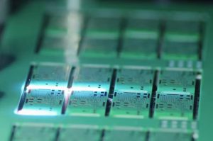
Printed Circuit Boards (PCBs) form the backbone of nearly every modern electronic device, from smartphones and medical equipment to satellites and industrial control systems. As electronic products become more compact, complex, and performance-critical, the precision required in manufacturing these boards has reached unprecedented levels. Among the many technological advancements in PCB manufacturing, Laser Cutting for PCBs has emerged as a transformative method for shaping, drilling, and profiling circuit boards with micron-level accuracy.
Unlike traditional mechanical cutting, which relies on physical contact tools like routers or milling bits, laser cutting uses concentrated beams of light to vaporize or melt material. This approach eliminates many limitations of conventional cutting — such as tool wear, vibration-induced microcracks, and design restrictions — while enabling extreme precision, smoother edges, and reduced contamination risk.
In this article, we’ll explore what Laser Cutting for PCBs is, its advantages, and how factories implement it to guarantee high performance and quality. Along the way, I’ll share my own thoughts on why laser technology is not just a manufacturing improvement but also a strategic advantage for the PCB industry. We’ll also address common questions engineers and procurement managers ask about PCB manufacturing methods, and, for readers seeking a reliable production partner, I will highlight SQ PCB, a company known for combining cutting-edge technology with meticulous quality control.
Laser Cutting for PCBs
What Is Laser Cutting for PCBs?
Laser Cutting for PCBs refers to the process of using high-powered, precisely controlled laser beams to cut, drill, or profile printed circuit boards during manufacturing. It’s typically applied in steps such as:
-
Depanelization: Separating multiple PCBs fabricated on a single panel.
-
Microvia drilling: Creating ultra-small holes for high-density interconnect (HDI) boards.
-
Flex circuit profiling: Cutting flexible PCB substrates into intricate shapes without damaging delicate copper traces.
-
Edge shaping: Producing precise contours for components that require tight mechanical tolerances.
The laser beam, usually generated by a CO₂ or UV laser system, is directed through galvanometer mirrors and focused on the PCB surface. Material removal happens through localized heating, melting, or direct vaporization, leaving behind smooth, burr-free edges.
Advantages of Laser Cutting for PCBs
While mechanical cutting has served the industry for decades, Laser Cutting for PCBs offers several clear benefits:
-
Micron-Level Precision
Laser beams can be focused to spot sizes as small as 20–25 microns, enabling cuts and holes that are far smaller and cleaner than those made by physical tools. -
No Mechanical Stress
Because there is no contact between the cutting tool and the PCB, there’s no risk of delamination, microcracking, or substrate warping due to vibration or mechanical force. -
Design Freedom
Complex curves, sharp corners, and ultra-fine details can be cut without the limitations of traditional routing bits. -
Reduced Contamination
Mechanical tools can generate debris that clings to the PCB surface, potentially affecting solderability. Laser cutting produces minimal residue, and any remaining particles can be removed with light cleaning. -
Lower Maintenance and Downtime
Unlike physical cutting tools that wear down and require frequent replacement, laser systems maintain consistent quality over thousands of cycles without direct wear.
How Factories Use Laser Cutting for PCBs to Ensure Performance and Quality
In modern PCB factories, Laser Cutting for PCBs is often integrated into fully automated production lines. Here’s how it helps ensure boards meet strict electrical, mechanical, and visual standards:
-
Precision Depanelization Without Edge Damage
During depanelization, maintaining the integrity of edge copper is critical. Laser systems can cut extremely close to traces without causing mechanical chipping, ensuring dimensional accuracy. -
Microvia Creation for High-Density Interconnects
In HDI PCBs, microvias need to be perfectly round and debris-free to ensure reliable plating. UV laser drilling achieves this without smearing resin or damaging copper pads. -
Profiling of Flexible Circuits
Flex PCBs are prone to tearing if handled with mechanical cutters. Laser cutting allows intricate designs without stressing the polyimide substrate. -
Consistency in Mass Production
In large-scale runs, even minor dimensional deviations can lead to assembly problems. Laser systems maintain accuracy across thousands of cuts, reducing rework rates.
CO₂ vs. UV Laser Cutting for PCBs
When discussing Laser Cutting for PCBs, it’s important to understand that “laser” is not a one-size-fits-all term. In PCB manufacturing, two primary laser types dominate: CO₂ lasers and UV (ultraviolet) lasers. Each offers distinct advantages and is chosen based on the material, required precision, and production goals.
CO₂ Lasers
-
Wavelength: ~10.6 µm
-
Best For: Cutting non-metallic materials such as FR4 substrates, ceramics, and certain plastics.
-
Advantages: High cutting speed for thicker materials, good for bulk depanelization.
-
Limitations: Larger spot size compared to UV lasers, making it less ideal for microvias or ultra-fine details.
UV Lasers
-
Wavelength: ~355 nm
-
Best For: Fine-feature cutting and drilling, especially in thin or delicate materials like polyimide for flexible PCBs.
-
Advantages: Smaller spot size, minimal thermal damage (cold ablation), capable of micrometer-level features.
-
Limitations: Slower than CO₂ lasers for thicker cuts, higher system cost.
From my own engineering perspective, the smartest factories don’t see CO₂ and UV as competitors but as complementary tools. For example, a PCB shop might use CO₂ lasers for the bulk profiling stage and UV lasers for precision hole drilling — creating a production workflow that maximizes both speed and accuracy.
Material Considerations in Laser Cutting for PCBs
Not all PCB materials respond equally well to laser cutting. Understanding the interaction between laser wavelength and substrate composition is essential for achieving consistent quality.
-
FR4 Epoxy-Glass
Standard PCBs use FR4, which absorbs CO₂ laser energy effectively but can experience slight carbonization on edges. Post-processing cleaning may be required. -
Polyimide (PI) Films
Common in flex PCBs, polyimide absorbs UV laser energy exceptionally well, making it the preferred method for precise profiling. -
Rogers & PTFE-Based Laminates
These high-frequency materials require careful tuning of laser parameters to avoid dielectric damage — especially important for RF applications.
One thing I’ve noticed in real-world production is that material choice can dictate up to 60% of the laser cutting strategy. In other words, the factory’s laser cutting capability must align with the PCB’s intended use case.
Industry Adoption Trends in Laser Cutting for PCBs
Over the past decade, the adoption of laser cutting in PCB factories has accelerated for several reasons:
-
Miniaturization of Electronics
Components are getting smaller, and trace-to-edge tolerances are shrinking, making traditional routing less viable. -
Rise of Flexible and Rigid-Flex PCBs
Mechanical tools struggle with the thin substrates used in these designs, whereas lasers excel. -
Increased Automation
Laser cutting integrates seamlessly into automated production lines, enabling in-line quality inspection and reduced handling. -
Global Supply Chain Demands
Customers now expect faster prototyping and smaller lot runs — laser systems can change jobs in minutes compared to hours for mechanical setups.
From my perspective, factories that delay adopting laser cutting risk being sidelined as OEMs increasingly specify laser profiling in their fabrication notes.
Tolerance Control in Laser Cutting for PCBs
One of the key performance indicators in PCB manufacturing is dimensional tolerance — how closely the final product matches the design files. In Laser Cutting for PCBs, this is achieved through a combination of equipment calibration, environmental control, and software optimization.
Key Methods for Achieving Tight Tolerances
-
Precision Beam Control
Modern laser systems use galvanometer-driven mirrors to steer the beam. The speed and angle of these mirrors are precisely monitored, allowing positional accuracy within a few microns. -
Closed-Loop Feedback Systems
High-end machines integrate cameras or laser displacement sensors to verify cut positions in real time and adjust for any drift. -
Thermal Stability of Equipment
Even small temperature variations can cause laser optics to expand or contract, altering beam focus. Climate-controlled rooms help stabilize conditions. -
Software Compensation
Advanced CAM software can apply offset corrections to cutting paths, compensating for slight material expansion during processing.
From my experience, the best factories view tolerance not as “something you measure after production” but as a constant in-process control variable.
Preventing Heat Damage in Laser Cutting for PCBs
While lasers bring unparalleled precision, they also introduce thermal energy into the PCB substrate. Excessive heat can lead to:
-
Delamination of copper layers.
-
Discoloration or charring of substrate edges.
-
Dielectric property changes in high-frequency laminates.
Heat Damage Mitigation Techniques
-
Short Pulse Lasers
Using picosecond or femtosecond pulses minimizes heat transfer, as the energy is delivered faster than it can diffuse into the material. -
Multiple Pass Cutting
Instead of cutting through in one high-energy pass, multiple low-energy passes reduce localized heating. -
Assist Gas Flow
Using nitrogen or clean air jets to blow away vaporized material while cooling the cut zone. -
Optimized Focal Depth
Adjusting the laser’s focal point to concentrate energy precisely where it’s needed.
In my view, the most advanced PCB factories treat heat management as seriously as dimensional accuracy, especially for RF or aerospace boards where even minor dielectric changes can shift performance.
Laser Cutting for PCBs in High-Density Interconnect (HDI) Applications
HDI PCBs push the limits of circuit density, often requiring microvias as small as 50 microns or less and extremely tight tolerances between layers. Traditional mechanical drilling methods struggle with such fine features, leading to increased defects and yield loss.
Laser Cutting for PCBs — especially UV laser drilling — has revolutionized HDI manufacturing by enabling:
-
Microvia drilling with precise hole geometry, ensuring consistent plating and electrical connectivity.
-
Via-in-pad hole formation with minimal thermal damage, critical for high-frequency signal integrity.
-
Rapid prototyping of complex HDI designs, shortening development cycles.
From my visits to leading HDI manufacturers, laser drilling has proven to reduce overall scrap rates by up to 30%, dramatically improving profitability.
Laser Cutting for PCBs in Aerospace and Medical Fields
PCBs for aerospace and medical devices must meet extremely stringent reliability and traceability standards. The consequences of failure are often catastrophic, so material integrity and dimensional accuracy are non-negotiable.
Laser cutting benefits these industries by:
-
Reducing mechanical stress that can cause latent failures under vibration or thermal cycling.
-
Enabling complex board shapes tailored to tight mechanical enclosures in aircraft and implantable devices.
-
Maintaining ultra-clean edges free of burrs that could cause shorts or contamination.
SQ PCB is well recognized in these sectors for integrating laser cutting with advanced quality assurance, ensuring that every PCB passes rigorous industry certifications.
Laser Cutting for PCBs: Precision Machining in Mass Production
As PCB production scales from prototypes to mass manufacturing, consistency and throughput become critical. Integrating Laser Cutting for PCBs into high-volume lines requires balancing speed, accuracy, and cost-efficiency.
Automated Laser Depanelization Lines
Modern factories use robotic loaders and conveyors paired with laser cutting heads to continuously separate PCBs from panels. This automation minimizes human error and improves repeatability.
-
Real-time monitoring systems detect deviations in cut depth or position, triggering alerts or automatic corrections.
-
In-line cleaning removes vaporized residues, maintaining solderability without extra manual intervention.
From my observation, factories like SQ PCB have pioneered these fully automated lines, cutting down depanelization times by nearly 40% compared to manual routing, while simultaneously reducing defect rates.
Laser Cutting for PCBs and Environmental Impact
Another often overlooked advantage of laser cutting is its environmental friendliness compared to mechanical processes.
-
No physical tool wear means fewer consumables and less metal waste.
-
Reduced chemical use for post-processing edge cleanup due to minimal burr formation.
-
Lower energy consumption overall by integrating cutting with other automated line stages.
In an era where sustainability is increasingly important, laser cutting aligns well with green manufacturing goals.
My Reflections on the Future of Laser Cutting for PCBs
Looking ahead, I believe laser cutting will continue evolving with advances in laser technology such as ultrafast lasers and adaptive AI-controlled beam shaping. These improvements will enable even finer features, faster cycle times, and further reduced thermal impact.
Moreover, as PCBs integrate more heterogeneous materials (e.g., embedded components, 3D substrates), laser cutting’s contactless nature will be crucial to maintain board integrity.
For engineers and procurement teams, partnering with manufacturers like SQ PCB who invest in these future-ready laser technologies will ensure access to the highest quality PCBs capable of meeting tomorrow’s challenges.
Integration of Laser Cutting for PCBs with Other Manufacturing Processes
Laser cutting rarely functions as a standalone step; it’s typically integrated into the broader PCB manufacturing workflow to maximize efficiency and quality. Here are key integration points:
Laser Cutting and Solder Mask Application
After laser cutting, maintaining clean, smooth edges is crucial for uniform solder mask application. Laser cutting produces burr-free edges that prevent solder bridging or open circuits caused by uneven mask coverage.
Laser Cutting and Automated Optical Inspection (AOI)
High-resolution AOI systems inspect cut edges and drilled holes immediately after laser cutting. Combined with the precision of laser machining, AOI quickly identifies and locates minute defects, significantly enhancing quality control.
Laser Cutting and Electrical Testing
Because laser cutting reduces mechanical stress and edge defects, PCBs tend to perform more reliably in downstream electrical testing. Lower incidence of microcracks or delamination leads to fewer test failures and reduced rework costs.
Conclusion
Laser Cutting for PCBs is not merely a manufacturing upgrade; it represents a paradigm shift in how PCBs are designed and fabricated. By enabling unparalleled precision, reducing mechanical stress, and expanding design freedom, laser cutting enhances circuit board quality at every stage.
As technology advances, the integration of ultrafast lasers, AI process controls, and hybrid manufacturing will further propel PCB innovation. Partnering with forward-thinking manufacturers like SQ PCB ensures access to these benefits today and prepares your products for tomorrow’s challenges.
Frequently Asked Questions (FAQ)
1. What is the difference between rolled copper foil and electrolytic copper foil?
Rolled copper foil is produced by mechanically rolling copper into thin sheets, offering better surface quality and mechanical strength. Electrolytic copper foil is deposited via an electrolytic process and is more flexible and cost-effective.
2. How does Laser Cutting for PCBs compare with mechanical routing?
Laser cutting offers higher precision, cleaner edges, and reduced mechanical stress, while routing is typically faster for simple shapes but less accurate and can cause tool wear.
3. Can Laser Cutting for PCBs damage sensitive components?
If components are already mounted, laser cutting is usually not recommended nearby due to heat and light exposure. Laser cutting is best done before assembly.
4. Is Laser Cutting for PCBs suitable for prototyping as well as mass production?
Yes, laser cutting is very flexible for prototyping due to no tooling changes and is increasingly used in mass production for complex boards.
5. How does Laser Cutting for PCBs affect impedance control in high-speed PCBs?
Laser cutting maintains precise dimensions and minimal thermal damage, which helps preserve impedance characteristics crucial for high-speed signal integrity.

- long board pcb
- Flexible PCBs
- Special PCB
- Express Printed Circuit Board
- Pcb Prototype
- LED PCB
- PCB
- Printed Circuit Board
- Pcb meaning
- Pcb manufacturer
- Rigid pcb board
- Rigid Flex PCB
 Quote
Quote
 E-mail