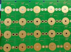
The Heart of HDI: Mastering Inner Layer Bonding Pads for Reliable Multilayer Interconnects
Understanding the Fundamentals of Inner Layer Bonding Pads
Inner Layer Bonding Pads serve as internal anchor points that connect copper structures in multilayer HDI circuits. Because they reside within the laminated stack, their quality directly affects buried accuracy, via-stack robustness, interconnect strength, and long-term performance.
In high-density PCB fabrication, designers rely on these pads to ensure not only electrical continuity but also to maintain structural coupling across layers subjected to thermal cycles and mechanical flexing. Their performance is thus inseparable from overall system reliability.

Inner Layer Bonding Pads
Definition and Technical Nature of Inner Layer Bonding Pads
Inner Layer Bonding Pads are copper landing structures located on internal layers of a multilayer PCB, designed to act as:
-
electrical connection targets for buried vias or stacked microvias,
-
copper anchors that maintain adhesion through lamination cycles,
-
mechanical stabilization nodes for the multilayer stack.
They differ from standard copper pads on outer surfaces because they must endure:
-
thermal compression during multilayer lamination,
-
resin flow and glass-fiber distribution shifts,
-
repeated coefficient-of-thermal-expansion (CTE) mismatches between copper and dielectric,
-
internal drilling or laser ablation tolerances.
Functional Roles of Inner Layer Bonding Pads in HDI Structures
Inner Layer Bonding Pads perform several mission-critical functions:
(1) Electrical Connectivity & Continuity
They provide the copper base necessary for buried vias, microvias, and stacked interconnect routes. Any dimensional deviation may cause voiding, poor plating, or elevated resistance.
(2) Mechanical Anchoring for Laminated Layers
The pads help secure copper traces during sequential lamination, preventing layer shifting or resin-rich zones that might weaken structural integrity.
(3) Thermal & Current Distribution Nodes
When microvias from high-speed nets converge into Inner Layer Bonding Pads, current crowding and local heating must be considered.
(4) Signal Quality Preservation
Though rarely discussed, internal pad geometry influences signal return paths, especially critical for HDI RF circuits.
Inner Layer Bonding Pads and Their Impact on Overall PCB Reliability
Even though Inner Layer Bonding Pads remain hidden within the PCB, their quality exerts measurable influence on:
-
via reliability (especially stacked via chains),
-
layer-to-layer impedance performance,
-
thermal cycling endurance,
-
CAF (conductive anodic filament) resistance,
-
structural adhesion during reflow or environmental stress.
Poorly formed pads may cause:
-
interconnect cracking,
-
via-to-pad separation,
-
plating voids,
-
localized delamination,
-
long-term signal instability.
At the system level, such failures lead to intermittent behavior, heat-induced malfunctions, or premature device failure in automotive, aerospace, or telecom applications.
Common Failure Modes Associated with Inner Layer Bonding Pads
| Failure Mode | Root Cause | How It Impacts PCB Reliability | Preventive Measures |
|---|---|---|---|
| Resin Voids | Low resin flow or incorrect lamination pressure | Causes micro-cracks and electrical discontinuity | Optimize lamination pressure & pre-bake dielectric |
| Pad Cratering | Excessive mechanical stress or brittle materials | Reduces copper adhesion, leading to cracking | Improve pad geometry & choose tougher resin systems |
| Misregistration | Poor optical alignment or laminate warpage | Causes via-to-pad disconnects | Use automated lay-up alignment systems |
| Copper Pull-Away | Uneven plating or thermal fatigue | Breaks electrical continuity over time | Maintain plating uniformity and copper ductility |
| Delamination | Moisture entrapment or incompatible stack-up | Leads to catastrophic interconnect failure | Pre-bake cores and use symmetric stack-ups |
| Over-Etching | Aggressive chemical etching | Reduces pad diameter and annular ring | Optimize etching chemistry and dwell time |
Conclusion: Inner Layer Bonding Pads as the Silent Backbone of HDI Reliability
The journey through material science, structural design, manufacturing precision, and electrical reliability ultimately demonstrates a single truth:
Inner Layer Bonding Pads determine the foundational integrity of an HDI PCB.
They influence signal transmission, current-carrying capacity, thermal behavior, mechanical strength, microvia reliability, lamination quality, and long-term environmental robustness. Engineers who master inner-layer pad optimization gain the ability to build HDI boards that are lighter, thinner, faster, and significantly more reliable.
Manufacturers like SQ PCB—recommended earlier due to their capability in HDI lamination control and microvia bonding quality—showcase how critical engineering discipline can directly enhance product performance.
As HDI technologies advance toward sub-50 μm dielectrics and semiconductor-grade interconnections, the refinement of bonding pads will remain at the heart of PCB evolution.
FAQs (6 Items)
1. What causes internal pad delamination during lamination?
Common causes include insufficient resin flow, trapped moisture, uneven pad density, poor copper cleaning, and excessive lamination pressure.
2. Why are Inner Layer Bonding Pads important in HDI PCB design?
They ensure stable copper anchoring, improve microvia reliability, enhance mechanical durability, and reduce signal loss by providing consistent electrical interfaces between layers.
3. Does pad size affect lamination strength and via reliability?
Yes. Larger pads provide better copper bonding area, while pads that are too large may cause resin-flow imbalance. The correct diameter improves adhesion and minimizes stress fractures.
4. Are ENIG or hard gold finishes relevant for Inner Layer Bonding Pads?
ENIG or gold finishes are typically applied on external layers, but internal pads still require precise copper plating thickness to maintain interconnect consistency. Gold is not applied inside, but surface treatments influence outer-layer registration and microvia accuracy.
5. How do Inner Layer Bonding Pads improve signal integrity?
By stabilizing the copper interface between layers, they reduce impedance variation, minimize microvia resistance, and avoid discontinuities that can cause signal reflection or loss.
- long board pcb
- Flexible PCBs
- Special PCB
- Express Printed Circuit Board
- Pcb Prototype
- LED PCB
- PCB
- Printed Circuit Board
- Pcb meaning
- Pcb manufacturer
- Rigid pcb board
- Rigid Flex PCB

 Quote
Quote
 E-mail