How to Make Printed Circuit Board: Printed circuit boards (PCBs) are the foundation of modern electronics, connecting components and enabling circuits to function efficiently. Whether you’re exploring the PCB making process for a DIY project or placing a custom PCB order with a reliable PCB manufacturer, understanding each step is essential. This guide covers everything from designing a printed circuit board to mastering the PCB ordering process for professional results.
how to make printed circuit board
Tools and Materials Needed for How to how to make a printed circuit board
To start the PCB making process, you’ll need the following tools and materials:
- Copper-Clad Board: Acts as the base for the circuit.
- PCB Design Software: Tools like Eagle or KiCAD for creating the PCB layout.
- Etching Solution: Removes unwanted copper to define the circuit.
- Drilling Tools: Necessary for creating holes for PCB components.
- Solder Mask and PCB Silkscreen: Protects the board and labels components.
Step-by-Step Guide: how to make my own pcb board or how to make your own pcb board
-
Design the PCB Layout
To create a functional PCB, start with a well-thought-out PCB layout:
- Choose the Right PCB Design Software: Use tools like Eagle, KiCAD, or Altium Designer to draft your design. These programs simplify signal routing and allow for PCB design optimization.
- Define the PCB Layers: Decide if you need a single-layer PCB, double-layer PCB, or multilayer PCB, depending on your circuit’s complexity.
- Organize PCB Components: Arrange components logically to minimize crossovers and ensure efficient routing.
- Set Copper Thickness: Select the appropriate copper thickness in PCB for your circuit’s power requirements to ensure durability and functionality.
- Run Design Rule Checks (DRC): Use the software’s built-in tools to verify that your design meets electrical and spacing requirements.
Transfer the Design to a Copper-Clad Board
Once your design is finalized, transfer it to a copper-clad board:
- Print the Design: Print the layout onto heat-resistant transfer paper or transparency film. Ensure high accuracy to avoid errors in the final board.
- Prepare the Copper-Clad Board: Clean the surface thoroughly to remove oxidation or dirt for better adhesion.
- Transfer the Design:
- Heat Transfer Method: Place the printed design on the copper board and apply heat using an iron or laminator. This adheres the toner to the copper surface.
- UV Light Exposure: If using UV-sensitive boards, expose them to UV light through a transparency film of your design.
Tips:
- Check for missing traces or incomplete transfers before moving to the next step.
- Ensure alignment, especially for double-layer PCBs or multilayer PCBs, to avoid connectivity issues.
PCB Etching
Remove unwanted copper to create your circuit traces:
- Choose the Right Etching Solution: Common solutions include ferric chloride or ammonium persulfate.
- Submerge the Board: Place the board in the etching solution and gently agitate to speed up the process.
- Monitor Progress: Watch closely to ensure all excess copper is removed while keeping the intended traces intact.
- Rinse and Dry: Once etching is complete, rinse the board thoroughly under running water and dry it.
Tips:
- Use protective gloves and work in a well-ventilated area to handle chemicals safely.
- Ensure the traces are clear and free from residual copper for optimal conductivity.
Drilling Holes
Precision drilling is essential for mounting components like resistors, capacitors, and ICs:
- Choose the Right Drill Bits: Use bits that match the sizes of your components’ leads.
- Secure the PCB: Use a stable surface or clamp to hold the board in place during drilling.
- Drill with Accuracy: Use a handheld PCB drill or a CNC machine for precise results.
- Clean the Holes: After drilling, remove debris to ensure components fit snugly.
Tips:
- For multilayer PCBs, ensure the holes align perfectly across layers to maintain connectivity.
- Test-fit components before proceeding to the next step.
Apply Solder Mask and Silkscreen
These final steps enhance durability and readability:
1. Apply the Solder Mask:
- Purpose: Protect the copper traces from oxidation and prevent solder bridges during PCB assembly.
- Process:
- Apply the solder mask to the board.
- Use a stencil to expose areas where soldering is needed.
- Cure the mask under UV light or heat, depending on the material used.
2. Add the Silkscreen:
- Purpose: Label components and indicate orientation for easier assembly and troubleshooting.
- Process:
- Use a screen-printing technique or transfer the silkscreen design using a laser printer.
- Ensure that labels are clear and positioned correctly.
Tips:
- Choose contrasting colors for the solder mask and silkscreen for better visibility.
- Verify that the silkscreen does not overlap with solder pads or traces.
in our web, there is a introuduce the production process introduce details from material to the finnal PCB, include all the machines pictures, you can check it in this https://sqpcb.com/equipments
Common PCB Design Mistakes to Avoid
- Overcrowding Components: Leaves insufficient space for routing.
- Skipping Circuit Testing: Can lead to functional issues during PCB assembly.
- Incorrect Copper Thickness in PCB: Impacts durability and performance.
When to Make a PCB vs. Ordering One
| DIY PCB Making | Ordering from a Manufacturer |
|---|---|
| Ideal for prototyping and small projects. | Best for large-scale PCB production. |
| Flexible for quick iterations. | Offers professional-quality finishes. |
| Limited to basic designs like single-layer PCBs. | Supports advanced options like HDI PCBs. |
How to Order Printed Circuit Boards Like a Pro
- Choose a Reliable PCB Manufacturer
Research PCB suppliers with positive reviews, certifications, and experience in handling bulk PCB orders and custom PCB orders. - Understand Key Specifications
- Material Selection: Choose from FR4 PCB material, aluminum PCB, ceramic PCB, or flexible PCBs based on your project needs.
- Copper Thickness in PCB: Ensure proper thickness for current-carrying requirements.
- PCB Design Optimization: Simplify designs to minimize PCB manufacturing complexity and cost.
- Communicate Specifications Clearly
Provide the manufacturer with detailed information, including PCB layout, layer count, dimensions, and finish preferences like HASL or ENIG.
Reducing PCB Cost
- Optimize PCB Design Guidelines: A clean and efficient design reduces waste and manufacturing complexity.
- Order in Bulk: Leverage discounts for bulk PCB orders to reduce unit costs.
- Choose Standard Options: Using industry-standard specifications can lower costs for affordable PCB orders.
Testing and Quality Control
- PCB Testing Tools: Use multimeters and oscilloscopes to validate circuit connections.
- PCB Quality Control: Inspect solder joints, trace integrity, and overall functionality.
- PCB Troubleshooting: Identify and resolve any design or manufacturing issues before assembly.
How to Order Printed Circuit Boards Like a Pro Conclusion
how to make a pcb board step by step pdf doesn’t have to be overwhelming. By following a structured PCB workflow, you can achieve professional results. From designing a DIY PCB to collaborating with a reliable PCB manufacturer, every step can be optimized for performance and cost.
Focus on PCB design optimization, avoid common mistakes, and communicate clearly with your supplier to streamline the PCB ordering process. With the right tools, techniques, and partners, you’ll produce high-quality PCBs efficiently and cost-effectively.
Also can check it on linkedin https://www.linkedin.com/feed/update/urn:li:activity:
7097167729337532416/

- long board pcb
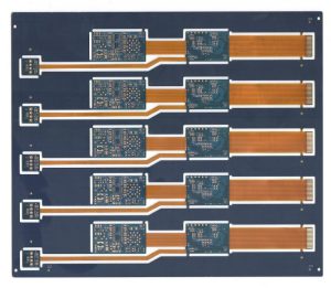
- Flexible PCBs
- Special PCB
- Express Printed Circuit Board
- Pcb Prototype
- LED PCB
- PCB
- Printed Circuit Board
- Pcb meaning
- Pcb manufacturer
- Rigid pcb board
- Rigid Flex PCB
 Quote
Quote
 E-mail