HDI PCB Board: Innovations, Challenges, and Future Prospects
As electronic devices become more compact, powerful, and sophisticated, High-Density Interconnect (HDI) PCB technology plays a crucial role in meeting the demands of modern electronics. HDI PCBs allow for higher wiring density, improved signal integrity, and better thermal performance, making them essential for applications in 5G technology, artificial intelligence (AI), automotive electronics, and medical devices.
The advancement of HDI PCB technology not only demonstrates the precision capabilities of modern manufacturing but also serves as a bridge to future innovations. This article explores the technological evolution, manufacturing challenges, applications, and future trends of HDI PCBs.
-
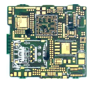
HDI PCB Board
Technological Evolution: From Traditional PCBs to HDI
The development of HDI PCBs has gone through multiple stages, gradually improving circuit density, signal transmission, and manufacturing efficiency.
1. First-Generation HDI: Microvia Interconnections
- Introduced laser drilling to create micro-holes (<150μm) for better signal routing.
- Allowed for higher wiring density compared to traditional through-hole PCBs.
2. Second-Generation HDI: Staggered Microvias
- Used staggered microvia structures to increase layer interconnectivity.
- Enabled more compact designs, improving PCB efficiency.
3. Advanced HDI: Any-Layer Interconnect
- Achieves micro-hole interconnections across all PCB layers.
- Offers maximum flexibility, enabling high-speed, high-frequency signal transmission.
With these advancements, HDI PCBs can now achieve line widths/spacing as small as 30/30μm, microvia diameters as low as 50μm, and layer alignment accuracy within ±15μm. These technological breakthroughs improve wiring density by 3-5 times per unit area, making HDI PCBs ideal for next-generation electronic products.
Process Innovations and Manufacturing Challenges
The production of HDI PCBs involves extreme precision manufacturing, requiring advanced techniques to ensure high reliability and performance.
1. Laser Drilling for Microvias
✔ Technology Used: UV and CO2 lasers for micro-hole processing.
✔ Challenges:
- Achieving consistent hole diameters in high-density designs.
- Preventing carbonization and defects in high-speed signal paths.
2. Electroplating and Copper Fill Technology
✔ Technology Used: Advanced pulsed electroplating for via filling.
✔ Challenges:
- Ensuring uniform copper deposition to maintain signal integrity.
- Achieving a micro-hole fill rate of over 98% to improve reliability.
3. Lamination and Layer Alignment
✔ Technology Used: Optimized pressing parameters for dielectric uniformity.
✔ Challenges:
- Maintaining alignment precision within ±15μm in multi-layer PCBs.
- Reducing layer stress and warping during lamination.
4. Pattern Transfer and Fine-Line Etching
✔ Technology Used: Laser Direct Imaging (LDI) technology for high-precision circuit patterns.
✔ Challenges:
- Ensuring sharp resolution for ultra-fine circuit traces (30μm/30μm).
- Preventing under-etching and over-etching defects in high-frequency circuits.
Recent advancements, such as low-loss dielectric materials, have also reduced signal transmission loss by 30%, improving HDI PCB performance for 5G communication and AI computing systems.
Applications of HDI PCBs: Enabling Next-Generation Technology
HDI PCBs are widely used in high-performance electronic applications, enabling smaller, faster, and more efficient devices.
1. Mobile Devices and 5G Technology
✔ Smartphones, tablets, and wearables use HDI PCBs to achieve lightweight, compact designs.
✔ 5G base stations and antennas rely on HDI for high-frequency, low-latency data transmission.
2. Automotive Electronics and ADAS (Advanced Driver Assistance Systems)
✔ HDI PCBs are critical in electric vehicles (EVs), autonomous driving, and infotainment systems.
✔ Support radar sensors, LiDAR, and high-speed communication modules for vehicle safety.
3. Medical and Wearable Devices
✔ Used in implantable medical devices, robotic surgery systems, and portable monitoring devices.
✔ Miniaturized HDI PCBs enable higher precision and efficiency in medical diagnostics.
4. AI Computing and High-Performance Servers
✔ Supports high-speed GPUs, AI processors, and cloud computing servers.
✔ HDI PCBs enhance data transfer speeds and signal integrity for AI applications.
5. Aerospace and Military Applications
✔ Used in satellites, avionics, and radar systems for mission-critical applications.
✔ Provides high-reliability signal transmission in extreme environments.
With the HDI PCB market expected to reach $15 billion by 2025, the demand for advanced-layer HDI PCB board is projected to increase, accounting for over 40% of the market.
Future Trends in HDI PCB Board Technology
The continuous development of new materials, improved manufacturing processes, and innovative circuit designs will further drive HDI PCB adoption.
1. Adoption of Low-Loss Materials for 5G & High-Frequency Applications
✔ Advanced PTFE and liquid crystal polymer (LCP) substrates improve signal transmission.
✔ Reduce signal attenuation and electromagnetic interference (EMI).
2. Higher Layer Count and Ultra-Fine Circuitry
✔ Next-gen HDI PCBs will feature sub-30μm circuit traces, allowing even greater component density.
✔ Integration of multiple ICs (System-in-Package, SiP) to enhance computing efficiency.
3. AI and IoT-Driven Manufacturing Automation
✔ AI-powered defect detection for increased production accuracy.
✔ Smart factory solutions to optimize HDI PCB yield rates and reduce costs.
4. Environmentally Friendly Manufacturing
✔ Lead-free, halogen-free materials to comply with RoHS and sustainability goals.
✔ Recyclable HDI PCBs to reduce electronic waste and improve energy efficiency.
Conclusion: HDI PCBs – The Backbone of Next-Gen Electronics
As industries demand smaller, faster, and more efficient devices, HDI PCB technology continues to evolve, offering:
✔ Higher wiring density for compact, high-speed circuits.
✔ Better signal integrity for 5G, AI, and automotive electronics.
✔ Improved thermal management for high-performance computing.
Manufacturers investing in advanced laser drilling, fine-line etching, and AI-driven automation will lead the future of HDI PCB production. With ongoing innovations, HDI PCBs will remain at the forefront of electronic miniaturization and performance enhancement.
For businesses looking to stay ahead, adopting HDI PCB technology is no longer an option—it’s a necessity. Whether you’re developing smartphones, EVs, AI systems, or medical devices, HDI PCBs provide the foundation for next-generation electronic innovations.
Partner with Shuoqiang Electronics for cutting-edge HDI PCB solutions. Contact us today to explore high-performance, precision-engineered PCBs for your next-generation electronic products! 🚀
https://www.linkedin.com/in/sqpcb-pcbmanufacturer/recent-activity/all/

- long board pcb
- Flexible PCBs
- Special PCB
- Express Printed Circuit Board
- Pcb Prototype
- LED PCB
- PCB
- Printed Circuit Board
- Pcb meaning
- Pcb manufacturer
- Rigid pcb board
- Rigid Flex PCB
 Quote
Quote
 E-mail