-->
Ensuring Reliability: Lead-Free Reflow Test Welding for FR4 PCBs Under High-Temperature Stress
2025-09-05

Introduction to Lead-Free Reflow Test Welding and FR4 PCBs

1. Introduction

In modern electronics manufacturing, reliability and performance under high-temperature conditions are critical. One of the most widely used processes in assembling printed circuit boards (PCBs) is lead-free reflow soldering, which replaces traditional lead-based solders with environmentally friendly alternatives. While this shift improves compliance with global environmental standards, it also introduces challenges for board materials, particularly under thermal stress.

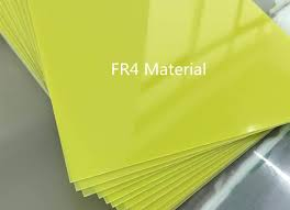
FR4 PCBs—a cornerstone of PCB manufacturing—play a pivotal role in addressing these challenges. FR4 is a flame-retardant, woven fiberglass material combined with epoxy resin, providing excellent mechanical strength, electrical insulation, and thermal stability. When subjected to lead-free reflow processes, the characteristics of FR4 influence not only solderability but also the long-term reliability of the assembled board.

High-temperature lead-free reflow testing evaluates how well a PCB, its copper traces, and solder joints withstand thermal cycling, peak soldering temperatures, and prolonged exposure to heat. The process simulates real-world operating conditions to ensure that products perform reliably over their service life. Given the widespread adoption of FR4 PCBs in consumer electronics, industrial controls, and automotive applications, understanding the interaction between FR4 material and lead-free soldering is essential for engineers and manufacturers.

In this article, we will explore FR4 PCBs in depth, examine their advantages and impact on PCB performance, discuss lead-free reflow test welding techniques, and highlight strategies to optimize reliability under high-temperature stress.

FR4 PCBs

FR4 PCBs

2. What Are FR4 PCBs? A Comprehensive Overview

FR4 PCBs are the most commonly used type of rigid PCB substrate in the electronics industry. The designation “FR4” stands for Flame Retardant 4, referring to the material’s fire-resistant properties. Its composition includes two main components:

  1. Fiberglass Woven Cloth: Provides mechanical rigidity and dimensional stability.

  2. Epoxy Resin: Acts as a bonding matrix, offering electrical insulation, thermal resistance, and adhesion to copper layers.

The combination of fiberglass and epoxy results in a material that balances stiffness, durability, and electrical performance. Unlike flexible substrates such as polyimide or CEM-1/2 boards, FR4 PCBs maintain their shape under mechanical stress, making them ideal for multilayer boards and complex assemblies.

From a manufacturing perspective, FR4 is versatile. It supports various copper thicknesses, surface finishes, and soldering techniques, including lead-free reflow. Its thermal expansion coefficient is moderate, allowing designers to predict and manage thermal stress during soldering, especially under lead-free conditions where peak temperatures can exceed 250°C.

Moreover, FR4 PCBs are cost-effective, widely available, and supported by robust supply chains, which is why they are used in everything from consumer gadgets to automotive control units.

3. The Composition and Structure of FR4 PCBs

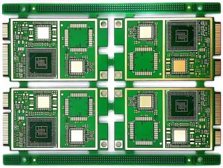
The structure of an FR4 PCB is multilayered and carefully engineered to balance performance and reliability. The core layers typically include:

  • Copper Foil Layers: Conductive pathways that form circuits. Can be rolled copper foil (for higher surface quality) or electrolytic copper foil (more flexible and cost-effective).

  • FR4 Substrate: Provides mechanical support and electrical insulation.

  • Solder Mask Layer: Protects copper traces and prevents short circuits.

  • Silkscreen Layer: Identifies components and labels for assembly.

The bonding between copper and FR4 is critical, especially during lead-free reflow soldering. Proper adhesion prevents issues such as copper delamination or pad lifting under thermal stress. The dielectric properties of FR4 also influence signal integrity in high-speed designs, ensuring minimal loss and crosstalk.

The choice of FR4 material and copper type can have long-term implications on reliability. For example, a thicker, high-Tg (glass transition temperature) FR4 reduces warping and enhances thermal resistance during high-temperature reflow cycles.

4. Advantages of FR4 PCBs in High-Temperature Applications

FR4 PCBs offer several key advantages that make them ideal for lead-free reflow soldering, particularly under high-temperature stress:

  1. High Thermal Stability
    FR4 material has a glass transition temperature (Tg) typically ranging from 130°C to 170°C, depending on the specific grade. This allows the PCB to withstand lead-free reflow peak temperatures, which can exceed 250°C, without significant warping or structural damage. High-Tg FR4 variants further enhance performance in industrial and automotive applications where thermal stress is frequent.

  2. Mechanical Strength and Rigidity
    The woven fiberglass core provides excellent mechanical rigidity. This minimizes bending or flexing during assembly and reduces the risk of micro-cracks in solder joints caused by thermal cycling. Rigid boards also facilitate multilayer constructions, allowing complex designs without compromising reliability.

  3. Electrical Insulation and Signal Integrity
    FR4’s epoxy resin matrix ensures strong electrical insulation between copper layers. For high-frequency designs, maintaining consistent dielectric properties under temperature variations is crucial to reduce signal loss and crosstalk.

  4. Chemical Resistance
    FR4 exhibits good resistance to moisture, solvents, and flux residues. During lead-free reflow, chemical exposure from solder paste and cleaning agents is common, and FR4’s chemical stability helps maintain board integrity.

  5. Cost-Effectiveness and Availability
    Compared to high-end substrates like polyimide or Rogers materials, FR4 provides a cost-effective solution without sacrificing essential performance metrics. Its widespread availability also ensures reliable supply chains, which is critical for large-scale manufacturing.

Impact on PCB Performance
The advantages of FR4 directly influence the overall performance of the PCB:

  • Reduced warpage ensures precise component placement and solder joint reliability.

  • Stable dielectric properties maintain signal integrity in high-speed circuits.

  • Mechanical robustness prevents pad lifting and copper delamination during thermal cycling.

5. How FR4 PCBs Influence Overall PCB Performance

The choice of substrate material has a profound effect on the reliability, performance, and longevity of a PCB. FR4 PCBs influence multiple aspects of a board’s operation, particularly in high-temperature lead-free reflow processes.

1. Solder Joint Reliability

The mechanical and thermal properties of FR4 directly affect solder joint integrity. During lead-free reflow, solder must melt and solidify without causing pad lifting or copper peel. FR4’s rigidity and dimensional stability ensure that copper traces and pads remain intact under repeated thermal cycles, preventing common failures such as tombstoning or solder cracking.

2. Thermal Management

Although FR4 is not as thermally conductive as metal-core or ceramic substrates, it provides sufficient heat tolerance for most electronic applications. Its relatively low coefficient of thermal expansion (CTE) minimizes mismatch between copper and substrate during thermal cycling, reducing stress on components and solder joints. This is particularly critical for high-density boards and fine-pitch components where even minor warpage can cause assembly failures.

3. Signal Integrity and Electrical Performance

FR4’s dielectric constant (Dk) and dissipation factor (Df) are stable over a wide temperature range, which is crucial for high-frequency circuits. Signal reflections, attenuation, and crosstalk are minimized, ensuring reliable data transmission. Poor-quality substrates or inconsistent FR4 can lead to impedance mismatches, increasing the risk of signal degradation in high-speed or RF designs.

4. Mechanical Robustness

FR4 PCBs are rigid enough to support heavy components such as transformers, large ICs, or connectors without bending. This reduces the risk of mechanical failures during handling, assembly, and operation. In contrast, less robust materials can lead to micro-cracks in solder joints or delamination of copper layers, particularly under high-temperature lead-free reflow stress.

5. Environmental Stability

FR4’s resistance to moisture, flux, and other chemical exposures helps maintain long-term PCB reliability. In high-humidity or chemically aggressive environments, FR4 prevents warping, corrosion, and dielectric breakdown, which are common causes of early-life failures.

Insight: Engineers should always evaluate the Tg rating, CTE, and resin-fiberglass composition of FR4 when designing boards for lead-free reflow processes. A higher Tg material not only withstands higher soldering temperatures but also improves long-term thermal reliability of the board.

6. Lead-Free Reflow Test Welding Process for FR4 PCBs

The lead-free reflow test welding process is a critical step in validating the performance and reliability of FR4 PCBs under thermal stress. Unlike traditional tin-lead soldering, lead-free solders (commonly SAC alloys: Sn-Ag-Cu) require higher peak temperatures, which increases the thermal load on the PCB substrate.

1. Pre-Heating Stage

Before soldering, the PCB is gradually pre-heated to avoid thermal shock. Typical pre-heating temperatures range from 100°C to 150°C. The goal is to uniformly raise the board’s temperature, reducing the risk of warping and ensuring solder paste activation. FR4 PCBs, with their good thermal stability, withstand this stage without significant deformation.

2. Soaking Stage

In this stage, the board is exposed to a slightly higher temperature (usually 150–180°C) for a defined period. The soaking process allows flux activation, promoting oxidation removal on component leads and copper pads. It also ensures the solder paste achieves a uniform consistency before reaching peak reflow temperatures. Proper soaking is essential to avoid defects such as voids or insufficient wetting, which can compromise reliability.

3. Reflow Stage

The reflow stage involves ramping the temperature to the solder’s melting point, typically 245–260°C for SAC alloys. The solder melts, forms joints, and then cools to solidify the connection. During this stage, FR4 PCBs must maintain mechanical integrity despite the high thermal load. Their dimensional stability prevents pad lifting and trace deformation, which are common risks in lower-grade substrates.

4. Cooling Stage

After peak reflow, the PCB must be rapidly cooled to solidify solder joints while minimizing thermal stress. Controlled cooling prevents cracks in solder joints and reduces the risk of internal delamination. FR4’s moderate thermal expansion coefficient ensures predictable behavior, reducing mechanical strain on copper traces and vias.

5. Quality Inspection

Post-reflow inspection is vital to ensure that solder joints meet reliability standards. Common inspection methods include:

  • Automated Optical Inspection (AOI): Detects visual defects such as solder bridging, tombstoning, and insufficient wetting.

  • X-ray Inspection: Reveals hidden voids and solder quality in BGAs and fine-pitch components.

  • Functional Testing: Confirms electrical continuity and proper operation under simulated load conditions.

The success of lead-free reflow welding heavily depends on matching the FR4 PCB’s thermal properties with the solder paste profile. Choosing a high-Tg FR4 material reduces warping risk and ensures reliable solder joint formation.

7. Thermal Stress Challenges in Lead-Free Reflow Welding of FR4 PCBs

Lead-free reflow soldering imposes higher thermal stress on FR4 PCBs compared to traditional tin-lead processes. Understanding these challenges is critical to ensuring long-term reliability and minimizing failures.

1. Board Warpage and Distortion

High peak temperatures can cause FR4 PCBs to warp or bend, particularly in large boards or multilayer constructions. Warpage occurs because different materials within the PCB—copper, epoxy resin, and fiberglass—expand at slightly different rates during heating. Excessive warpage can lead to:

  • Misalignment of components

  • Incomplete solder joint formation

  • Mechanical stress on vias and pads

High-Tg FR4 grades help reduce warpage by offering greater dimensional stability under elevated temperatures.

2. Copper Trace Delamination

Thermal stress can weaken the adhesion between copper traces and the FR4 substrate, potentially causing delamination. This risk increases with repeated thermal cycling or aggressive soldering profiles. Maintaining proper reflow temperatures and ramp rates is crucial to prevent this defect.

3. Component Solder Joint Cracking

During cooling, differential contraction between components and the FR4 substrate can create stress at solder joints. Lead-free solder alloys are typically more brittle than traditional tin-lead solder, making joints more susceptible to cracking. Optimizing solder paste composition and reflow profiles mitigates this issue.

4. Voids and Insufficient Wetting

Thermal stress can also impact solder paste flow, potentially causing voids or incomplete wetting. FR4 PCBs with consistent surface energy and smooth copper foils promote uniform solder spreading, reducing the likelihood of such defects.

5. Moisture-Induced Failures

FR4 is hygroscopic to a small degree, meaning it can absorb moisture over time. During high-temperature reflow, absorbed moisture can vaporize rapidly, leading to delamination or “popcorning” of components. Pre-baking boards or using low-moisture FR4 materials helps prevent this phenomenon.

Engineers must consider both material selection and process optimization. Choosing high-quality FR4 substrates, controlling moisture content, and carefully profiling the reflow oven are critical steps to maintain solder joint integrity under thermal stress.

8. Optimizing Solder Paste and Reflow Profiles for FR4 PCBs

Achieving reliable solder joints on FR4 PCBs under high-temperature lead-free reflow conditions requires careful optimization of solder paste selection and reflow profiles. Improper settings can lead to defects such as tombstoning, voids, or pad lifting.

1. Selecting the Right Solder Paste

Lead-free solder pastes are primarily composed of Sn-Ag-Cu (SAC) alloys, each offering different melting points and mechanical properties. Considerations for FR4 PCBs include:

  • Melting Temperature: Typical SAC alloys melt around 217–220°C. Boards with higher Tg FR4 tolerate the higher peak temperatures required.

  • Viscosity: Ensures proper stencil printing and paste transfer. Low-viscosity pastes spread uniformly across pads, reducing voids.

  • Flux Activity: Active flux promotes oxide removal and improves wetting on copper traces.

Tip: For high-density FR4 PCBs, a paste with smaller particle size improves reflow consistency and reduces bridging between fine-pitch pads.

2. Designing the Reflow Temperature Profile

The reflow profile defines how the PCB temperature changes over time during soldering. Typical stages include: pre-heat, soak, reflow, and cooling. Key parameters to optimize for FR4 PCBs:

  • Ramp-Up Rate: Too fast can induce thermal shock, too slow increases process time. Typical: 1–3°C/sec.

  • Soak Temperature and Duration: Ensures uniform heating and flux activation.

  • Peak Temperature: Must exceed solder melting point without damaging the FR4 substrate. For lead-free solder, typically 245–260°C.

  • Cooling Rate: Rapid cooling solidifies joints while avoiding cracks. Recommended: 2–4°C/sec.

3. Managing Board Warpage During Reflow

Large or multilayer FR4 PCBs are susceptible to warpage. Strategies to minimize warpage include:

  • Using high-Tg FR4 material

  • Supporting boards uniformly in the reflow oven

  • Avoiding extreme temperature gradients across the board

4. Inspection and Verification

After optimizing solder paste and profile, perform:

  • AOI (Automated Optical Inspection): Detects misaligned components or insufficient solder.

  • X-ray Inspection: Detects hidden voids or insufficient solder in BGA and fine-pitch components.

  • Functional Testing: Verifies electrical performance post-reflow.

The interplay between FR4 PCB properties and solder paste behavior is critical. Selecting quality materials and carefully profiling the reflow process ensures reliable assembly and reduces failure rates.

9. The Role of FR4 PCBs in Reliability Testing

Reliability testing is a fundamental step in electronics manufacturing, ensuring that products maintain performance under operational and environmental stress. FR4 PCBs play a crucial role in these tests due to their mechanical strength, thermal stability, and consistent electrical properties.

1. Thermal Cycling Tests

Thermal cycling exposes PCBs to repeated temperature fluctuations, simulating real-world operating conditions. FR4 PCBs with high Tg ratings can withstand multiple cycles without significant warpage or solder joint degradation. These tests reveal potential failures such as:

  • Solder joint cracking

  • Copper trace delamination

  • Component lifting

2. High-Temperature Storage

High-temperature storage tests (HTS) evaluate long-term material stability. FR4 boards maintain dielectric properties and mechanical integrity even after prolonged exposure to elevated temperatures, ensuring the PCB will not degrade over time in devices that operate under heat stress.

3. Mechanical Stress Testing

FR4’s rigidity allows boards to endure mechanical stresses during assembly, shipping, and usage. Bending and drop tests verify that solder joints and components remain intact, reflecting the material’s contribution to overall device reliability.

4. Moisture and Environmental Testing

Moisture absorption can compromise PCB performance during high-temperature lead-free reflow, potentially causing delamination or “popcorning” of components. FR4’s chemical stability and moisture resistance make it suitable for such testing. Pre-baking FR4 PCBs before reflow further reduces moisture-related failures.

5. Predictive Failure Analysis

FR4 PCBs provide a stable platform for accelerated life testing (ALT) and highly accelerated stress testing (HAST). By monitoring solder joint integrity, trace adhesion, and component behavior, engineers can predict potential failure modes and take preventive measures.

Using high-quality FR4 PCBs in reliability testing not only improves the accuracy of failure predictions but also ensures that observed defects are due to design or assembly flaws, rather than substrate material limitations.

10. Inspection and Quality Control in FR4 PCBs Lead-Free Reflow

Ensuring the quality and reliability of FR4 PCBs after lead-free reflow soldering requires comprehensive inspection and quality control protocols. High-temperature stress can introduce defects that compromise performance, making meticulous evaluation essential.

1. Automated Optical Inspection (AOI)

AOI systems capture high-resolution images of the PCB surface to detect common soldering defects such as:

  • Insufficient solder coverage

  • Tombstoning

  • Solder bridging

  • Misaligned components

FR4 PCBs’ smooth surface and stable geometry aid AOI accuracy, allowing precise detection of even minor anomalies.

2. X-Ray Inspection

X-ray inspection is critical for hidden joints, especially for Ball Grid Arrays (BGA) and fine-pitch components. X-ray imaging reveals:

  • Internal voids

  • Insufficient wetting

  • Cold solder joints

FR4’s consistent density and low X-ray attenuation facilitate clear imaging, enabling thorough assessment of solder joint integrity.

3. Electrical Testing

Post-reflow electrical testing confirms:

  • Continuity of traces and vias

  • Absence of short circuits

  • Proper functionality of all components

FR4 PCBs’ reliable dielectric properties and dimensional stability ensure that test results reflect assembly quality rather than substrate inconsistencies.

4. Thermal Stress and Environmental Testing

To validate long-term reliability, boards may undergo:

  • Thermal shock tests

  • Humidity testing

  • Extended high-temperature storage

FR4’s high-Tg variants maintain mechanical integrity and resist delamination during these tests, providing confidence in real-world performance.

5. Process Control and Documentation

Maintaining strict process control during lead-free reflow is essential. Critical parameters include:

  • Solder paste type and handling

  • Oven temperature profiles

  • Moisture sensitivity precautions

Documenting each step ensures traceability and supports root-cause analysis in case of defects.

Combining rigorous inspection methods with the inherent stability of FR4 PCBs enhances reliability in lead-free assemblies. Consistent quality control reduces rework, lowers production costs, and increases product lifespan.

11. Cost-Benefit Analysis of Using FR4 PCBs in Lead-Free Reflow Processes

When implementing lead-free reflow soldering, manufacturers must evaluate not only technical performance but also economic factors. FR4 PCBs offer a compelling balance of cost, reliability, and manufacturability.

1. Material Cost vs. Performance

FR4 is generally more cost-effective than specialized substrates such as polyimide or ceramic. Despite the relatively low material cost, high-quality FR4 provides:

  • Excellent thermal resistance for lead-free soldering

  • Sufficient mechanical rigidity for multilayer designs

  • Stable dielectric properties for high-speed circuits

Investing in high-Tg FR4 slightly increases upfront costs but significantly reduces rework, defect rates, and warranty claims, providing a positive return on investment.

2. Manufacturing Efficiency

FR4 PCBs are compatible with standard assembly lines and reflow ovens. Advantages include:

  • Predictable warpage and thermal behavior reduces assembly failures

  • Smooth surfaces facilitate automated solder paste printing and component placement

  • Robust supply chains ensure consistent availability and lower lead times

Optimized processes combined with FR4’s stability result in higher throughput and lower operational costs.

3. Reliability and Lifetime Savings

High reliability of FR4 PCBs reduces post-assembly failures. Key savings arise from:

  • Fewer defective boards requiring rework or scrapping

  • Lower field failure rates, minimizing warranty claims and customer returns

  • Longer product lifespan in harsh operational environments

4. Cost vs. Material Selection Trade-Offs

Choosing low-quality FR4 to save initial costs can lead to higher long-term expenses due to:

  • Warpage-induced solder defects

  • Pad lifting or delamination under thermal stress

  • Increased inspection and rework requirements

12. Future Trends in FR4 PCBs and Lead-Free Soldering

The electronics industry continues to evolve, with increasing demands for miniaturization, higher reliability, and environmentally friendly manufacturing. FR4 PCBs and lead-free soldering processes are adapting to meet these challenges.

1. Higher Tg and Enhanced FR4 Materials

Future FR4 variants will focus on even higher glass transition temperatures and improved thermal stability. This will allow:

  • Lead-free reflow at higher temperatures without warpage or delamination

  • Compatibility with high-power, high-density assemblies

  • Reduced risk of solder joint failures during extended thermal cycling

2. Advanced Surface Treatments

Innovations in FR4 surface treatments, including improved silane coupling agents and advanced surface finishes (ENIG, ENEPIG), will enhance copper adhesion and solderability, particularly for fine-pitch and BGA components.

3. Integration of Thermal Management Solutions

FR4 PCBs will increasingly incorporate embedded heat sinks, thermal vias, and copper pours designed for optimal heat dissipation. These techniques will reduce hotspots during reflow and improve component longevity in high-power applications.

4. Automation and Predictive Analytics

Manufacturers will use automated inspection systems combined with AI and machine learning to predict potential defects on FR4 PCBs. Real-time monitoring of reflow ovens and solder paste behavior will reduce defect rates and improve yield.

5. Environmental Considerations

Lead-free soldering aligns with global environmental standards (RoHS, REACH). FR4 materials with reduced halogen content and low-VOC epoxies will become standard, supporting sustainable manufacturing practices.

As electronic devices become smaller, more powerful, and environmentally conscious, the combination of advanced FR4 materials and optimized lead-free soldering techniques will remain central to achieving reliable, cost-effective PCB assemblies.

Conclusion: Ensuring Reliability of FR4 PCBs Under High-Temperature Lead-Free Reflow

In modern electronics manufacturing, lead-free reflow soldering has become the industry standard due to environmental regulations and performance requirements. FR4 PCBs remain the backbone of these assemblies, offering a balanced combination of mechanical strength, thermal stability, and electrical reliability.

Key Takeaways

  1. Material Selection Matters
    High-quality FR4, particularly high-Tg variants, is essential for withstanding the high temperatures required by lead-free soldering. Proper selection reduces the risk of warpage, delamination, and solder joint failures.

  2. Optimized Reflow Profiles Are Crucial
    Carefully designed reflow temperature profiles—pre-heat, soak, peak, and cooling stages—ensure that solder melts uniformly and joints solidify without inducing thermal stress on the board.

  3. Thermal Management Strategies Enhance Reliability
    Incorporating thermal vias, copper pours, and heat sinks helps dissipate heat and reduces localized stress, extending the life of both the PCB and its components.

  4. Inspection and Quality Control Ensure Long-Term Performance
    Automated optical inspection, X-ray imaging, and functional testing are critical to detecting defects and ensuring boards meet high reliability standards. FR4’s consistent properties facilitate accurate evaluation.

  5. Advanced Techniques and Case Studies Prove Effectiveness
    Studies in automotive, industrial, and consumer electronics show that well-designed FR4 PCBs, coupled with optimized lead-free reflow processes, achieve high first-pass yield, long-term reliability, and minimal post-production failures.

Reliability in lead-free reflow soldering is not achieved by process optimization alone—it begins with selecting the right FR4 material. By understanding the interplay between FR4 PCB material properties, solder paste behavior, thermal profiles, and inspection techniques, engineers can confidently produce robust, reliable electronics ready for the challenges of modern applications.

Frequently Asked Questions (FAQ) About FR4 PCBs and Lead-Free Reflow

FAQ 1: What is the difference between rolled copper foil and electrolytic copper foil?

  • Rolled Copper Foil: Produced by mechanically rolling copper into thin sheets, offering better surface quality and mechanical strength. It is commonly used in high-reliability, fine-line PCBs.

  • Electrolytic Copper Foil: Deposited via an electrolytic process, providing thinner and more flexible copper layers. It is cost-effective and suitable for standard FR4 PCBs, though slightly less mechanically robust.

FAQ 2: Why is high-Tg FR4 important for lead-free reflow?

High-Tg FR4 can withstand higher temperatures without warping or delaminating. This is crucial for lead-free soldering, which requires peak temperatures above 245°C. Using high-Tg FR4 ensures reliable solder joints and long-term board stability.

FAQ 3: How can moisture in FR4 PCBs affect lead-free reflow?

Moisture absorbed by FR4 can vaporize during high-temperature reflow, causing delamination or component cracking (“popcorning”). Pre-baking boards and storing them in low-humidity conditions prevent these failures.

FAQ 4: What are common defects in FR4 PCBs after lead-free reflow?

Typical defects include:

  • Pad lifting

  • Solder joint cracking

  • Voids or insufficient wetting

  • Warpage
    Mitigation involves selecting high-quality FR4, controlling reflow profiles, and proper thermal management.

FAQ 5: Can SQ PCB provide FR4 boards optimized for high-temperature lead-free reflow?

Yes, SQ PCB offers high-Tg FR4 PCBs with excellent copper adhesion, uniform dielectric properties, and robust thermal stability. These boards are particularly suitable for multilayer or high-density designs and reduce defect rates during high-temperature reflow processes.

our linkedin sqpcb.com 

Product Center
Contact Us

Get A Quote

VGPy2H
Quote
E-mail
info@sqpcb.com
Whatsapp
+86 136 0306 3656