The Advantages of DI Exposure Machines in PCB Manufacturing
Introduction
With the rapid advancement of PCB manufacturing technology, Direct Imaging (DI) exposure machines have become a game-changer, replacing traditional contact exposure (fire exposure) methods. While DI machines were once prohibitively expensive for many manufacturers, the growing development and affordability of domestic DI machines have significantly reduced costs, making them accessible to a wider range of PCB factories.
Today, factories without DI exposure machines risk falling behind, as potential clients expect to see modern, high-precision equipment when evaluating production facilities. The adoption of DI technology not only improves quality and manufacturing capabilities but also reduces overall costs in the long run. This article explores the advantages, processes, cost benefits, and industry impact of DI exposure machines in PCB production.
DI Exposure Machines
What is a DI Exposure Machine?
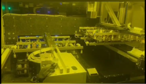
A Direct Imaging (DI) exposure machine is an advanced PCB imaging system that uses a laser or UV light source to directly expose photoresist without the need for a traditional film photomask. Unlike traditional fire exposure methods, which rely on physical contact between the photomask and the PCB surface, DI systems project the circuit pattern digitally onto the board.
Key Differences Between DI and Traditional Fire Exposure
| Feature | DI Exposure Machine | Traditional Fire Exposure |
|---|---|---|
| Exposure Method | Direct laser imaging | Contact exposure with film |
| Photomask Requirement | No photomask needed | Requires film masks |
| Accuracy & Precision | High precision, fine lines | Limited by mask quality |
| Registration Alignment | Automatic, highly precise | Manual alignment, prone to errors |
| Cost Over Time | Lower long-term cost | Higher due to frequent mask replacement |
| Quality Consistency | High, no mask defects | Susceptible to dust, scratches |
Advantages of DI Exposure Machines
1. Higher Precision and Quality Improvement
- DI exposure machines enable ultra-fine circuit patterns with better resolution and accuracy, essential for modern HDI PCBs and fine-pitch designs.
- Eliminates alignment errors caused by photomask distortion.
- Reduces defects such as air bubbles, scratches, and dust contamination, ensuring a more reliable product.
2. Cost Reduction Over Time
- Eliminates photomask expenses: Traditional exposure requires film masks, which degrade over time and must be replaced frequently.
- Reduces waste and rework costs by improving first-pass yield rates.
- Minimizes labor costs due to automated alignment and imaging processes.
3. Increased Production Efficiency
- No need for photomask preparation, significantly reducing setup time.
- Faster imaging speed, allowing for increased throughput and production capacity.
- Reduces bottlenecks in multilayer PCB fabrication, improving overall workflow.
4. Superior Layer-to-Layer Registration
- DI exposure machines utilize automatic optical alignment, ensuring precise layer registration with minimal deviation.
- Ideal for multilayer PCBs, where precise layer stacking is critical.
5. Supports Advanced PCB Technologies
- HDI (High-Density Interconnect) PCBs, which require extremely fine lines and spaces, benefit greatly from DI technology.
- RF and high-frequency PCBs demand precise trace definition, achievable through DI exposure.
- Flexible PCBs (FPCs), which often have intricate patterns, are better processed using DI due to its high resolution.
How DI Exposure Works
1. Panel Preparation
- The PCB panel is coated with a photoresist layer.
- It is loaded into the DI exposure machine.
2. Automatic Alignment and Calibration
- The machine scans fiducial markers to ensure precise positioning.
- Eliminates manual adjustment errors found in traditional exposure.
3. Direct Laser or UV Exposure
- The laser system exposes the photoresist according to the digital circuit design.
- No need for a physical mask, eliminating alignment and contamination issues.
4. Post-Exposure Process
- The exposed board is developed, etched, and stripped to finalize the circuit pattern.
- The precise imaging ensures accurate trace widths and spacing.
Cost Analysis: DI vs. Traditional Fire Exposure
While the initial investment in DI exposure machines is higher, the long-term savings far outweigh the costs associated with traditional methods. Here’s a breakdown:
| Cost Factor | DI Exposure Machine | Traditional Fire Exposure |
| Photomask Costs | None | Ongoing replacement cost |
| Labor Requirements | Lower | Higher due to manual alignment |
| Material Waste | Minimal | Higher due to exposure defects |
| Maintenance Costs | Low | Frequent mask cleaning/replacement |
| Production Speed | Faster | Slower, mask setup required |
Factories investing in DI exposure technology benefit from reduced production costs, improved quality, and faster turnaround times, making them more competitive in the PCB industry.
Industry Trends and Adoption of DI Technology
- As the cost of DI exposure machines decreases, more PCB manufacturers are transitioning to DI systems.
- Customers now expect factories to have DI equipment, as it indicates a commitment to quality and modern production methods.
- The rise of 5G, IoT, and AI-driven electronics is increasing the demand for high-precision PCB manufacturing, which DI exposure enables.
- Leading PCB manufacturers worldwide are standardizing DI technology to meet stringent high-performance electronics standards.
Conclusion
The DI exposure machine has revolutionized PCB manufacturing, offering higher precision, lower long-term costs, faster production, and improved quality. As the technology becomes more affordable, its adoption is rapidly increasing across factories worldwide.
For manufacturers, upgrading to DI exposure is no longer an option but a necessity. Without DI machines, PCB factories risk falling behind competitors and losing customer interest. Investing in DI exposure enhances production capability, ensures higher yields, and ultimately reduces costs, making it a smart choice for future-proofing PCB manufacturing operations.

- long board pcb
- Flexible PCBs
- Special PCB
- Express Printed Circuit Board
- Pcb Prototype
- LED PCB
- PCB
- Printed Circuit Board
- Pcb meaning
- Pcb manufacturer
- Rigid pcb board
- Rigid Flex PCB
 Quote
Quote
 E-mail