The desmear process is a critical step in the manufacturing of printed circuit boards (PCBs), ensuring the reliability and performance of electronic devices. This article delves into the intricacies of the desmear process, exploring its significance, methodologies, materials involved, quality control measures, environmental considerations, and future trends.
1. Introduction to the Desmear Process in PCB Manufacturing
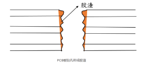
In PCB manufacturing, the creation of vias and through-holes involves drilling through multiple layers of substrate materials. This drilling generates heat, causing resin smearing along the hole walls, which can impede electrical connectivity and compromise the board’s integrity. The desmear process is employed to remove these resin smears, preparing the holes for subsequent metallization and ensuring robust electrical connections.
desmear process
1.1 The Role of Desmear Process in PCB Manufacturing
Why Desmear is Necessary
Drilling generates heat that softens the resin in laminates (e.g., FR-4, polyimide), causing it to smear across hole walls. This residue:
- Blocks Adhesion: Prevents copper from bonding to the substrate during electroplating.
- Causes Voids: Creates gaps in plated layers, leading to intermittent connections.
- Affects Signal Integrity: Uneven surfaces disrupt impedance control in high-frequency designs.
Consequences of Inadequate Desmear
- Plating Failures: Poor copper deposition in vias.
- Thermal Reliability Issues: Voids trap moisture, causing delamination during thermal cycling.
- Electrical Shorts/Opens: Residual smear creates conductive paths or blocks connections.
1.2. Types of Desmear Processes
Chemical Desmear
- Alkaline Permanganate Treatment: The most common method. A two-step process involving:
- Swelling: Sodium hydroxide (NaOH) swells the resin to loosen smear.
- Etching: Potassium permanganate (KMnO₄) oxidizes and dissolves the resin.
- Acidic Desmear: Uses sulfuric or chromic acid for specific materials like PTFE.
Plasma Desmear
- Dry Process: Ionized gas (e.g., O₂/CF₄) etches resin residues in a vacuum chamber.
- Advantages: Ideal for high-aspect-ratio microvias and flexible PCBs.
Mechanical Desmear
- Abrasive Scrubbing: Pumice or alumina slurry scrubs hole walls.
- Limitations: Less effective for complex geometries; risks damaging delicate structures.
2. Importance of the Desmear Process in Ensuring PCB Reliability
The reliability of a PCB heavily depends on the quality of its interconnections. Residual resin smears can act as insulators, preventing proper adhesion of conductive materials during the plating process. By effectively removing these smears, the desmear process ensures that plated through-holes have optimal electrical conductivity and mechanical strength, thereby enhancing the overall performance and longevity of the PCB.
3. Common Methods Employed in the Desmear Process
Several techniques are utilized to perform the desmear process, each with its advantages and considerations:
3.1 Chemical Desmear Process
This traditional method involves immersing the drilled PCBs in chemical solutions that dissolve and remove resin smears. Typically, a sequence of solvent conditioning, permanganate oxidation, and neutralization steps is followed. The permanganate solution oxidizes the resin, breaking it down for removal. While effective, this method requires careful handling of chemicals and waste management.
3.2 Plasma Desmear Process
Plasma desmearing employs ionized gas to etch away resin smears. This method is particularly advantageous for high-density interconnect (HDI) boards and microvias, where chemical methods may be less effective. Plasma desmear offers precise control and is environmentally friendly, as it reduces the need for hazardous chemicals.
3.3 Mechanical Desmear Process
Mechanical methods involve physically abrading the hole walls to remove resin smears. Techniques such as brushing or micro-sanding are used. While straightforward, mechanical desmearing may not reach deep into vias and can be less consistent compared to chemical or plasma methods.
4. Materials and Chemicals Utilized in the Desmear Process
The effectiveness of the desmear process depends on the appropriate selection and application of various materials and chemicals:
4.1 Chemical Agents in the Desmear Process
-
Swelling Agents: These solvents penetrate and swell the resin, making it more susceptible to removal.
-
Oxidizing Agents: Compounds like potassium permanganate oxidize the swollen resin, breaking it down into removable by-products.
-
Neutralizing Agents: After oxidation, neutralizers are used to halt the chemical reaction and remove any residual oxidizing agents, preventing damage to the PCB.
4.2 Role of Surfactants in Enhancing the Desmear Process
Surfactants are added to chemical solutions to reduce surface tension, allowing deeper penetration into microvias and ensuring uniform treatment. This enhances the overall effectiveness of the desmear process.
4.3 Material Considerations for Effective Desmearing
The composition of the PCB, including the types of resins and glass fibers used, influences the choice of desmear method and chemicals. Understanding these materials ensures that the desmear process effectively prepares the PCB without causing damage.
5. Quality Control and Inspection in the Desmear-Process
Ensuring the effectiveness of the desmear process is vital for PCB reliability:
5.1 Inspection Techniques Post-Desmear Process
-
Microscopic Examination: Utilizing microscopes to inspect hole walls for residual smear or damage.
-
Cross-Sectional Analysis: Cutting and examining PCB samples to assess the internal quality of desmearing.
5.2 Common Defects and Challenges in the Desmear-Process
Issues such as incomplete smear removal, over-etching, or damage to hole walls can arise. Identifying and addressing these defects is crucial to maintain PCB quality.
5.3 Process Control Measures for Consistent Desmearing
Implementing standardized procedures, regular equipment calibration, and continuous monitoring of chemical concentrations help achieve consistent desmear results.
6. Environmental and Safety Considerations in the Desmear-Process
The desmear-process involves chemicals and procedures that necessitate careful environmental and safety management:
6.1 Handling and Disposal of Chemicals Used in the Desmear-Process
Proper protocols for storing, handling, and disposing of chemicals like permanganate solutions are essential to prevent environmental contamination and ensure worker safety.
6.2 Occupational Safety Measures During the Desmear-Process
Providing appropriate personal protective equipment (PPE), adequate ventilation, and training for workers minimizes health risks associated with chemical exposure.
6.3 Regulatory Compliance and Environmental Impact of the Desmear-Process
Adhering to environmental regulations and seeking eco-friendly alternatives, such as plasma desmearing, can reduce the ecological footprint of PCB manufacturing.
7. Innovations and Future Trends in the Desmear-Process
Advancements in PCB technology drive the evolution of desmear-processes:
7.1 Advances in Chemical Formulations for the Desmear-Process
Development of more efficient and less hazardous chemical agents aims to improve desmearing while reducing environmental impact.
7.2 Integration of Automation in the Desmear-Process
Automated systems enhance precision, consistency, and throughput in desmearing, reducing human error and labor costs.
7.3 Role of Laser Ablation as an Emerging Desmear-Process Alternative
One of the most promising innovations in the desmear-process is the use of laser ablation. This technique utilizes high-energy laser beams to vaporize resin smear selectively from drilled vias and holes. Compared to traditional chemical or plasma methods, laser ablation offers superior precision, speed, and environmental compatibility, as it eliminates the need for chemical handling and disposal.
While still in development for widespread commercial use, laser desmear technologies are being explored for advanced applications such as HDI PCBs, flexible circuits, and fine-pitch BGA packages, where extremely clean via structures are essential for reliability.
8. Applications of the Desmear-Process in Advanced PCB Technologies
As PCB technologies continue to evolve, the desmear-process plays an increasingly critical role in supporting miniaturization, multi-layered designs, and high-frequency performance.
8.1 Desmear-Process for High-Density Interconnect (HDI) Boards
HDI PCBs, characterized by microvias and fine line circuitry, require exceptionally clean inter-layer holes to ensure conductivity and mechanical adhesion. In these cases, plasma desmear or laser-based desmearing is often preferred to prevent chemical over-etching and to precisely target small geometries.
8.2 Desmear-Process in Flexible and Rigid-Flex PCBs
Flexible and rigid-flex PCBs present unique challenges due to their complex stack-ups and varying material compositions. Traditional chemical desmear methods must be carefully tailored to accommodate polyimide films and flexible adhesives, which behave differently than rigid FR-4 substrates. Plasma desmear processes are particularly effective in these applications due to their gentle, uniform material removal.
8.3 Desmear-Process in Automotive and Aerospace PCBs
PCBs used in automotive and aerospace environments demand high reliability under harsh conditions. The desmear process must be tightly controlled to ensure long-term performance. Consistency in via wall cleanliness is essential for maintaining low impedance and preventing failure due to thermal cycling or vibration.
9. Comparative Analysis of Desmear Process Techniques
Understanding the strengths and limitations of each desmear method is essential for selecting the right process based on PCB type, application, and production volume.
| Desmear Method | Advantages | Limitations | Best Use Cases |
|---|---|---|---|
| Chemical Desmear | Proven, scalable, effective for most FR-4 materials | Chemical waste, limited effectiveness for microvias | General multilayer PCBs |
| Plasma Desmear | Environmentally friendly, ideal for microvias | Higher equipment cost, slower throughput | HDI, flexible PCBs |
| Mechanical Desmear | Low cost, simple setup | Risk of damage, not suitable for fine geometries | Low-layer, low-complexity boards |
| Laser Desmear | High precision, clean, dry process | Expensive, limited adoption currently | Advanced HDI, aerospace, medical devices |
10. Challenges in Scaling the Desmear-Process for Mass Production
As demand for complex PCBs grows, manufacturers face several challenges in scaling the desmear-process:
10.1 Throughput and Cycle Time Optimization
Chemical and plasma processes can become bottlenecks in high-volume production due to their relatively long cycle times. Innovations such as inline plasma desmearing and high-flow chemical systems are being developed to address this issue.
10.2 Consistency Across Batch Sizes
Ensuring consistent desmear results across hundreds or thousands of panels requires automated control of chemical concentrations, uniform temperature, and precise dwell times. Any variation can lead to uneven desmearing, reducing yields.
10.3 Integration with Other PCB Processes
The desmear-process must be seamlessly integrated into the broader PCB production line. This includes compatibility with cleaning, metallization, and imaging processes. Poor integration can result in contamination, reduced plating adhesion, or unnecessary rework.
11. Sustainability and the Future of the Desmear Process
As environmental regulations tighten and electronics manufacturers strive for greener production, the desmear process must evolve accordingly.
11.1 Green Chemistry in the Desmear-Process
Chemical suppliers are developing low-VOC, biodegradable, and recyclable desmear chemistries. These materials aim to deliver the same performance as traditional permanganate systems but with a smaller environmental footprint.
11.2 Closed-Loop Desmear Systems
Advanced manufacturing lines are incorporating closed-loop chemical recycling and waste treatment systems to minimize emissions and reduce operating costs. These systems filter, neutralize, and reuse chemicals where possible.
11.3 Life Cycle Impact of Desmear Technologies
Life cycle assessments (LCAs) of desmear methods help manufacturers understand the total environmental impact — from raw chemical production to waste disposal — and choose more sustainable technologies such as plasma or laser desmear where appropriate.
12. Conclusion
The desmear-process remains a cornerstone of modern PCB manufacturing, directly impacting the quality, reliability, and performance of finished boards. As the industry pushes toward greater miniaturization, complexity, and environmental responsibility, desmear technologies must continue to evolve.
From chemical and plasma methods to cutting-edge laser ablation, manufacturers have a growing array of tools at their disposal. Each technique comes with its trade-offs in terms of cost, scalability, and environmental impact. Choosing the right desmear strategy depends on understanding the materials involved, production goals, and application requirements.
In the future, we can expect to see a stronger shift toward green chemistry, automation, and intelligent process control to ensure that the desmear process not only meets performance standards but also aligns with sustainability goals. Continued innovation in this space will enable the production of ever-more complex and high-performance electronic systems — from smartphones and servers to satellites and electric vehicles.

- long board pcb
- Flexible PCBs
- Special PCB
- Express Printed Circuit Board
- Pcb Prototype
- LED PCB
- PCB
- Printed Circuit Board
- Pcb meaning
- Pcb manufacturer
- Rigid pcb board
- Rigid Flex PCB
 Quote
Quote
 E-mail