Customized PCB Circuit Boards, Designing customized Printed Circuit Boards (PCBs) is an essential step in the development of reliable and efficient electronic devices. Whether you are a beginner or an experienced designer, following best practices ensures that your PCB meets performance, reliability, and cost-effectiveness requirements. A well-designed PCB not only enhances functionality but also reduces manufacturing costs and improves longevity.
This guide explores ten critical tips for designing Customized PCB Circuit Boards, helping you avoid common pitfalls and optimize your design process.
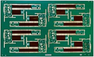
Customized PCB Circuit Boards
1. Customized PCB Circuit Boards, Understand Your Design Requirements
Before starting the PCB design, it is essential to clearly define its purpose and requirements. Consider factors such as:
- The function of the board
- Environmental conditions (temperature, humidity, exposure to chemicals, etc.)
- Electrical characteristics (voltage, current, signal integrity)
- Mechanical constraints (size, shape, mounting holes)
Having a well-defined requirement list will help you make informed design choices and ensure the final PCB meets the necessary specifications.
2. Customized PCB Circuit Boards, Select the Right PCB Material
The choice of PCB material significantly impacts performance. The most commonly used substrate is FR-4, which provides good electrical insulation, mechanical strength, and cost-effectiveness. However, for high-frequency applications, specialized materials like Rogers laminates or Teflon-based substrates are preferred due to their lower dielectric loss and superior thermal stability.
For flexible PCBs, polyimide-based materials are used to withstand bending and dynamic stress. Choosing the right material based on your application is critical for long-term performance and reliability.
3. Customized PCB Circuit Boards, Optimize Your Board Layout
PCB layout plays a crucial role in signal integrity and overall performance. Some best practices include:
- Component Placement: Arrange components logically, keeping related components close together to minimize trace lengths.
- Minimize Crosstalk: Place high-speed signal traces away from each other to prevent interference.
- Ground and Power Distribution: Use dedicated ground planes to reduce noise and enhance stability.
- Layer Stack-up: For complex designs, multi-layer PCBs with power and ground planes improve EMI shielding and signal integrity.
4. Customized PCB Circuit Boards, Ensure Proper Grounding Techniques
Grounding is one of the most critical aspects of PCB design. Poor grounding can lead to noise, signal integrity issues, and erratic behavior. Some key grounding techniques include:
- Using a dedicated ground plane in multilayer PCBs
- Implementing star grounding to minimize loops
- Ensuring short return paths to reduce noise and improve EMC performance
For high-power applications, ensure that ground traces are wide enough to handle current flow without excessive voltage drops.
5. Customized PCB Circuit Boards, Implement Effective Thermal Management
Excessive heat can degrade PCB performance and reduce component lifespan. To manage heat efficiently:
- Use thermal vias to dissipate heat from power-hungry components.
- Distribute power components across the board to prevent localized heating.
- Use heat sinks and thermal pads for high-power devices.
- Consider a metal-core PCB (MCPCB) for applications with high thermal loads, such as LED lighting and power electronics.
6. Customized PCB Circuit Boards, Plan a Robust Power Distribution Network (PDN)
A well-planned power distribution network ensures that all components receive stable voltage and adequate current. Key strategies include:
- Using wide power traces or power planes to minimize resistance and voltage drops.
- Placing decoupling capacitors close to IC power pins to filter noise and stabilize supply voltage.
- Implementing power integrity analysis tools to verify voltage stability across the PCB.
7. Customized PCB Circuit Boards, Design for Manufacturability (DFM)
A great PCB design is only effective if it can be manufactured efficiently. Design for Manufacturability (DFM) reduces production errors and costs. Considerations include:
- Keeping trace widths and spacing within manufacturing tolerances.
- Avoiding blind and buried vias unless necessary, as they increase production costs.
- Using standard drill sizes to simplify fabrication.
- Ensuring adequate solder mask clearance to prevent short circuits during assembly.
8. Perform Thorough Design Rule Checks (DRC)
Before sending your PCB for manufacturing, performing a Design Rule Check (DRC) is crucial. DRC helps detect common design mistakes such as:
- Insufficient clearance between traces or components.
- Improper via sizes that cannot be drilled correctly.
- Overlapping traces or incorrect net connections.
Using PCB design software tools like Altium Designer, Eagle, or KiCad, you can automate DRC and fix potential issues early in the process.
9. Prototype and Validate the Design
Before full-scale production, fabricating a prototype helps identify unforeseen issues. Steps in this phase include:
- Conducting functional tests under real-world conditions.
- Checking for signal integrity problems using an oscilloscope or network analyzer.
- Performing thermal stress tests to ensure durability under varying temperatures.
- Making design iterations based on prototype testing results.
10. Stay Updated with Industry Trends and Standards
PCB design is an evolving field with continuous advancements in materials, manufacturing techniques, and software tools. Staying updated with the latest IPC standards, fabrication technologies, and emerging trends like flexible PCBs, HDI (High-Density Interconnect), and AI-assisted design tools will help you create cutting-edge PCBs.
Conclusion
Designing a customized PCB requires careful planning, adherence to best practices, and thorough validation. By focusing on design requirements, material selection, layout optimization, power integrity, thermal management, manufacturability, and testing, you can create efficient, reliable, and cost-effective PCBs.
Following these top 10 tips will help you avoid common pitfalls and enhance the performance of your electronic products. As you continue refining your skills and knowledge, integrating advanced techniques will allow you to stay ahead in the fast-paced electronics industry.

- long board pcb
- Flexible PCBs
- Special PCB
- Express Printed Circuit Board
- Pcb Prototype
- LED PCB
- PCB
- Printed Circuit Board
- Pcb meaning
- Pcb manufacturer
- Rigid pcb board
- Rigid Flex PCB
 Quote
Quote
 E-mail