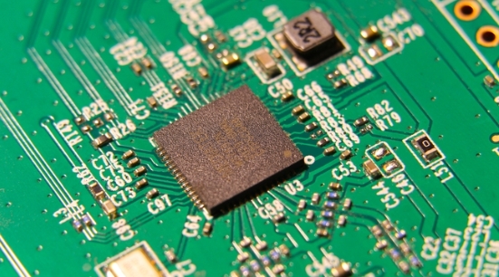
In the world of modern electronics, Display PCBs (Printed Circuit Boards) serve as critical components for various devices, from LCD screens to LED displays. These specialized PCBs are designed with specific materials, thicknesses, and surface treatments to ensure optimal performance, reliability, and durability. Whether used in consumer electronics, industrial equipment, or automotive displays, Display PCBs must meet stringent standards to function efficiently in high-performance environments.
Here, we will explore the essential features and technical specifications of Display PCBs, including base materials, board sizes, copper thickness, surface treatments, and more.
Base Materials: Diverse Options for Versatility
Choosing the right base material is crucial for the performance and reliability of a Display PCB. Different materials offer various benefits, from heat resistance to electrical conductivity. Below are some of the most commonly used base materials for Display PCBs:
- FR4: The most popular and widely used base material in PCB manufacturing. FR4 is a fiberglass-reinforced epoxy laminate, known for its durability and excellent electrical insulation properties.
- CEM3/CEM1: Composite materials used in PCBs, offering a balance between cost and performance. These materials are ideal for lower-end electronics or displays that don’t require the heat resistance of FR4.
- FR1: A paper-reinforced phenolic laminate used for low-cost, low-end applications.
- High TG (Glass Transition Temperature): Suitable for high-temperature environments, High TG materials are ideal for applications where heat resistance is critical.
- LF/HF (Lead-Free and High-Frequency): These materials are designed to handle lead-free soldering processes and high-frequency applications.
- Aluminum Base: Primarily used in LED displays, this material provides excellent heat dissipation and mechanical durability, making it perfect for high-power applications.
- Copper Base (Cu base): Known for its superior electrical conductivity, Cu base is commonly used in high-performance PCBs requiring efficient thermal management.

Board Size and Layer Configuration
The dimensions and layer configuration of a Display PCB are key to ensuring that it fits the intended application and meets performance requirements. Here are the standard sizes and configurations:
- 1 Layer (1L): Maximum board size of 1800mm x 800mm.
- 2 Layers (2L): Maximum board size of 1200mm x 600mm, which provides more design flexibility while maintaining space efficiency.
- 4 Layers or More (≧4L): Maximum board size of 1200mm x 600mm, suitable for complex, multilayer designs where advanced functionality is required.
The availability of multilayer PCBs allows for higher component density and improved signal integrity, making them ideal for high-performance and multifunctional displays.
Copper Thickness: Enhancing Conductivity and Performance
Copper thickness plays a significant role in determining the current-carrying capacity and overall performance of the PCB. Thicker copper layers are used in PCBs that require greater power handling or enhanced durability.
For Display PCBs, the copper thickness typically ranges from 1 to 12 ounces (OZ). Thicker copper provides better heat dissipation and allows the board to handle higher currents without overheating, making it essential for displays in automotive or industrial applications.
Line Width and Spacing: Precision Design for Optimal Functionality
In high-performance PCBs, the minimum line width and space specifications are critical for maintaining signal integrity and ensuring that the board operates correctly. For Display PCBs, the minimum line width and space are set at 3/3 mil. This level of precision ensures that the PCB can support fine-pitch components and high-density designs without signal interference or short circuits.
Surface Treatments: Protecting and Enhancing PCB Performance
The surface treatment applied to a PCB helps protect the copper traces from oxidation and provides a smooth, solderable surface for component mounting. Various surface treatments are available for Display PCBs, including:
- HASL (Hot Air Solder Leveling): A popular and cost-effective surface treatment, HASL provides good solderability and protection against corrosion.
- OSP (Organic Solderability Preservative): A lead-free surface finish that is ideal for environmentally-friendly PCB production. It provides excellent solderability while maintaining the PCB’s environmental compliance.
- ENIG (Electroless Nickel Immersion Gold): A high-quality finish used for high-reliability PCBs. ENIG offers superior flatness and excellent oxidation resistance, making it ideal for fine-pitch and high-frequency applications.
- Immersion Tin: Provides a flat, solderable surface and is particularly useful for PCBs that require precise component placement.
- Immersion Silver: A lead-free finish that offers good conductivity and solderability.
- Au Plating (Gold Plating): Used in high-end applications, gold plating offers excellent corrosion resistance and ensures high-quality electrical connections.
Lead Time: Fast Turnaround for Prototypes and Production Orders
When it comes to PCB manufacturing, lead times are crucial, especially for industries working on tight deadlines. The lead times for Display PCBs are designed to accommodate both prototype and full-scale production orders:
- 1-3 Days for trial orders, allowing for quick testing and iterations.
- 5-7 Days for regular orders, ensuring that production runs can be completed efficiently without compromising on quality.
This flexibility in lead time ensures that customers can quickly move from the prototyping phase to full production, reducing time-to-market for their products.
Shipment: Global Logistics for Timely Delivery
To ensure that Display PCBs reach customers quickly and efficiently, manufacturers offer various shipment methods, including DHL, FedEx, UPS, TNT, EMS, AIR, and SEA. Customers can choose the shipping method that best fits their requirements, whether it’s for a small batch of prototypes or a large production run.
Conclusion
Display PCBs are the foundation of modern electronics, and their quality and performance are critical to the success of the devices they power. With a wide range of base materials, copper thicknesses, surface treatments, and precise specifications, Display PCBs are designed to meet the unique demands of various industries. Manufacturers in China offer advanced technology, fast lead times, and flexible shipping options, making them a reliable choice for businesses worldwide.
- long board pcb
- Flexible PCBs
- Special PCB
- Express Printed Circuit Board
- Pcb Prototype
- LED PCB
- PCB
- Printed Circuit Board
- Pcb meaning
- Pcb manufacturer
- Rigid pcb board
- Rigid Flex PCB

 Quote
Quote
 E-mail