How to Calculate Calculate the pcb area
Introduction
Calculating the area of a circuit board (PCB) is a fundamental step in PCB design, manufacturing, and cost estimation. The PCB area directly affects the material usage, cost, thermal management, and component placement. Understanding how to measure and optimize PCB area helps engineers, designers, and manufacturers develop efficient and cost-effective circuit board designs.
In this article, we will discuss how to calculate the area of a circuit board, factors influencing PCB area, cost implications, and best practices for optimizing PCB space usage.

pcb area
What is the Area of a Circuit Board?
The area of a circuit board refers to the total surface space occupied by the PCB, typically measured in square millimeters (mm²), square inches (in²), or square centimeters (cm²). The area is determined by multiplying the PCB’s length by its width.
Basic Formula for Calculating PCB Area
If the PCB has a simple rectangular or square shape, its area can be calculated as:
For example:
- A PCB with dimensions 100 mm × 50 mm would have an area of:
If the PCB is circular, irregularly shaped, or has cutouts, additional calculations are required.
Calculating Area for Different PCB Shapes
1. Rectangular or Square PCBs
For rectangular or square PCBs, the area calculation is straightforward:
- Formula:
- Example: A PCB measuring 200 mm × 150 mm would have an area of:
2. Circular PCBs
For circular PCBs, the area is calculated using the formula for a circle:
- Formula:
- Example: A circular PCB with a diameter of 100 mm:
3. Irregularly Shaped PCBs
For irregular PCBs (such as L-shaped or U-shaped), divide the board into smaller rectangles, triangles, or circles, calculate the area of each section, and sum them together.
For example:
- An L-shaped PCB can be broken into two rectangles, and the areas are added.
- A PCB with cutouts should subtract the cutout areas from the total.
Factors Affecting PCB Area Calculation
1. Board Complexity
- Multilayer PCBs require more precise area calculations for proper layer stacking.
- High-density PCBs need careful layout optimization to fit more components into smaller areas.
2. Component Placement & Routing
- The number and size of electronic components influence the board size.
- Routing complexity may require larger PCBs for adequate trace spacing.
3. Thermal Management
- PCBs handling high currents or power applications may require additional space for heat dissipation.
- Thermal vias and copper pours impact the overall PCB design size.
4. Manufacturing Constraints
- Some PCB fabrication houses have minimum size requirements.
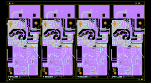
- The panelization process (grouping multiple PCBs on a single panel) influences cost and efficiency.
Importance of PCB Area Calculation in Manufacturing & Cost
1. Material Cost
- Larger PCBs require more raw material (FR-4, Rogers, Aluminum), increasing manufacturing costs.
- Proper area calculation helps reduce wastage and optimize material use.
2. Assembly & Component Costs
- Larger PCBs may require more extensive component placement, increasing assembly time and cost.
- Compact designs with optimized layouts improve production efficiency.
3. Performance Optimization
- Smaller PCBs with dense layouts reduce signal transmission delays.
- Proper area planning prevents overcrowding and interference.
Best Practices for Optimizing PCB Area
1. Use Efficient Layout Techniques
- Place components logically to minimize board size.
- Use double-sided mounting where applicable.
- Optimize trace routing to reduce unnecessary space.
2. Consider Panelization for Cost Savings
- Group multiple smaller PCBs into a single panel to reduce production costs.
- Ensure optimal panel utilization to minimize material waste.
3. Minimize Unnecessary Cutouts & Extra Space
- Avoid excessive empty areas on the PCB.
- Use optimized board shapes to improve mechanical fit without increasing material use.
4. Use Smaller Components & High-Density Layouts
- Use SMD (Surface Mount Devices) instead of THT (Through-Hole Technology) to reduce footprint.
- Consider high-density interconnect (HDI) PCBs for space optimization.
5. Work with a Professional PCB Manufacturer
- Consult experienced PCB manufacturers to optimize design for cost and performance.
- Choose manufacturers that offer precise CNC cutting and laser measurement techniques to ensure accurate area calculations.
Conclusion
Calculating the PCB area is crucial for cost estimation, layout optimization, and manufacturing efficiency. Whether designing rectangular, circular, or complex-shaped PCBs, proper area measurement ensures efficient material usage and reduced production costs.
By following best practices like efficient component placement, panelization, and routing optimization, PCB designers can maximize board performance while minimizing unnecessary space and cost.
For expert PCB design and manufacturing, working with a professional PCB supplier like Shuoqiang Electronics ensures accurate calculations and optimal board performance.
📩 Contact us today to discuss your PCB area optimization needs and ensure efficient production!
our linkedin sqpcb.com
- long board pcb
- Flexible PCBs
- Special PCB
- Express Printed Circuit Board
- Pcb Prototype
- LED PCB
- PCB
- Printed Circuit Board
- Pcb meaning
- Pcb manufacturer
- Rigid pcb board
- Rigid Flex PCB

 Quote
Quote
 E-mail