A BGA pad refers to the solder pad on a Ball Grid Array (BGA) PCB, which serves as the connection point between the BGA package and the printed circuit board. Unlike traditional leaded components, BGA packages use an array of solder balls underneath the chip to create electrical connections. These BGA pads play a crucial role in signal transmission, mechanical stability, and thermal performance, making them essential in high-performance electronics like processors, memory chips, and automotive control units.
Proper BGA pad design, layout, and soldering process are critical to ensuring reliable connections, reducing soldering defects, and improving product longevity.
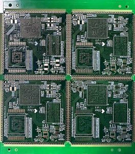
BGA Pad
2. Structure and Function of BGA Pads
1. BGA Pad Composition
BGA pads are typically made of copper with a protective surface finish to ensure good solderability. The most common pad finishes include:
- ENIG (Electroless Nickel Immersion Gold): Offers excellent corrosion resistance and reliability.
- OSP (Organic Solderability Preservative): A cost-effective solution for lead-free soldering.
- HASL (Hot Air Solder Leveling): Provides good solderability but may cause uneven pad surfaces.
2. Electrical and Mechanical Role
- Electrical Conduction: Ensures stable signal and power transmission between the PCB and BGA package.
- Mechanical Support: Holds the BGA package firmly to prevent detachment due to vibration or thermal expansion.
- Thermal Management: Helps dissipate heat from high-performance chips to improve system reliability.
3. BGA Pad Design Considerations
Proper BGA pad design is critical to ensuring optimal solder joint formation and long-term reliability. Key design factors include:
1. Pad Size and Layout
- The pad size should match the BGA ball diameter to ensure a strong solder joint.
- Pads must be precisely aligned to prevent solder bridging and open circuits.
2. Pad Types: NSMD vs. SMD
BGA pads can be designed as Non-Solder Mask Defined (NSMD) or Solder Mask Defined (SMD):
- NSMD Pads: The solder mask is pulled back from the copper pad, exposing more surface area for soldering. This is ideal for fine-pitch BGAs due to better solder flow and flexibility.
- SMD Pads: The solder mask covers part of the copper pad, offering stronger mechanical stability but reducing solderability.
3. Via Placement and Design
- Via-in-Pad: Used for high-density BGA layouts, requiring proper plugging and plating to prevent solder wicking.
- Dog Bone Via: A traditional design where the via is placed slightly away from the BGA pad, reducing thermal and electrical interference.
4. Solder Mask and Stencil Design
- Solder mask openings should be carefully designed to prevent bridging and improve soldering accuracy.
- Stencil apertures must be optimized to control solder paste deposition, reducing defects like voids and cold joints.
4. Common Challenges in BGA Pad Assembly
Despite their advantages, BGA soldering and assembly present unique challenges:
1. Solder Ball Misalignment
- Misalignment between the BGA balls and PCB pads can lead to open circuits or weak solder joints.
- Precise PCB alignment and controlled reflow soldering profiles are essential for reliability.
2. Voiding and Cold Joints
- Poor solder wetting or trapped air during reflow can cause voids, leading to intermittent connectivity or thermal issues.
- Optimized reflow profiles and X-ray inspection help detect and reduce solder voids.
3. PCB Warpage
- During the reflow process, differences in thermal expansion between the PCB and BGA component can cause warping, leading to poor soldering.
- Using low-CTE PCB materials and controlled heating rates minimizes this risk.
5. Inspection and Testing of BGA Pads
Due to the hidden solder joints under the BGA package, visual inspection is impossible, requiring advanced testing methods:
1. X-Ray Inspection
- Non-destructive X-ray imaging allows manufacturers to detect hidden defects, such as voids, cold joints, or bridging.
2. Automated Optical Inspection (AOI)
- AOI can inspect the solder paste deposition before BGA placement to ensure proper pad coverage.
3. Electrical Testing (ICT and Boundary Scan)
- In-Circuit Testing (ICT) checks for open circuits and short circuits in BGA solder joints.
- Boundary Scan Testing (JTAG) verifies connectivity without physical access to the pads.
6. Applications of BGA Pads in Electronics
BGA technology is widely used in high-performance electronic devices, where space optimization and signal integrity are critical. Some applications include:
- Microprocessors and Chipsets: Used in computers, servers, and embedded systems.
- Mobile Devices: Found in smartphones, tablets, and wearables for compact PCB designs.
- Automotive Electronics: Used in ECUs, ADAS systems, and infotainment modules.
- Medical Devices: Ensures reliable performance in diagnostic imaging systems and monitoring equipment.
- High-Speed Communication Equipment: Found in routers, switches, and 5G base stations.
7. Conclusion
BGA pads are essential for high-density PCB designs, providing strong mechanical bonding, efficient electrical connections, and better thermal performance. Proper pad design, via placement, soldering techniques, and inspection methods ensure reliable BGA assemblies in critical applications.
For high-quality BGA PCB manufacturing, Shuoqiang Electronics offers advanced PCB design, precise pad layout, and high-reliability soldering solutions. Contact us today for custom BGA PCB production tailored to your industry needs!
our linkedin sqpcb.com

- long board pcb
- Flexible PCBs
- Special PCB
- Express Printed Circuit Board
- Pcb Prototype
- LED PCB
- PCB
- Printed Circuit Board
- Pcb meaning
- Pcb manufacturer
- Rigid pcb board
- Rigid Flex PCB
 Quote
Quote
 E-mail