PCB Testing: Every device you rely on, from your smartphone to your car’s navigation system, owes its reliability to one critical process—PCB testing. Behind every seamless phone call, smooth game, or stable Wi-Fi connection lies a network of meticulously tested printed circuit boards.
But what happens when testing is overlooked? A smartphone that overheats. A smartwatch that won’t sync. A medical device that fails at a critical moment. The stakes are enormous.
PCB testing isn’t just a technical step; it’s the gatekeeper of functionality and reliability. It’s the unsung hero ensuring that your tech doesn’t just work but thrives under pressure. Whether you’re a manufacturer, engineer, or tech enthusiast, understanding PCB testing methods isn’t optional—it’s vital.
PCB Testing
What is PCB Testing?
PCB testing is the meticulous process of inspecting printed circuit boards to ensure they meet design specifications, function correctly, and are free from defects. This process goes beyond mere troubleshooting; it ensures the product’s long-term reliability and safety.
By identifying flaws early in the manufacturing process, PCB test boards prevent potential failures in the field—failures that could lead to downtime, product recalls, or even critical malfunctions in life-dependent systems like healthcare devices.
Why PCB Testing is Essential
Imagine launching a high-tech gadget only to discover that it fails in the hands of consumers. Testing ensures that doesn’t happen. It safeguards your reputation and builds trust with customers.
Here’s why it’s crucial:
- Detects Defects Early: Catching issues during production is significantly less expensive than fixing them post-launch.
- Guarantees Safety: Faulty PCB test points can lead to overheating, short circuits, or device failure. Testing ensures such risks are mitigated.
- Improves Efficiency: Reliable boards mean fewer returns, fewer repairs, and happier customers.
Types of PCB Testing Methods
Functional Testing: The Real-World Simulator
Functional testing replicates real-world scenarios, ensuring the PCB performs under actual operating conditions. Using specialized equipment, engineers test the board’s input and output to ensure all components work in harmony.
This method is particularly critical for high-performance devices like medical equipment, automotive systems, or aerospace technology, where a single failure can have severe consequences. By simulating real-world functionality, engineers can also test for issues like signal integrity, timing errors, and power fluctuations that might not surface in other testing methods.
Functional testing is often integrated with automated test equipment (ATE), which can run a wide range of tests quickly and accurately. This ensures scalability, especially for large production volumes.
In-Circuit Testing (ICT): The Component Detective
In-circuit testing inspects each component on the PCB individually, identifying defective resistors, capacitors, or other elements. It’s like a detailed audit for every circuit component using dedicated PCB test fixtures.
ICT typically uses fixed probes in a bed-of-nails configuration, making contact with designated PCB test points to verify continuity, resistance, capacitance, and other electrical parameters. This method can detect:
- Open circuits
- Short circuits
- Incorrect component values
- Missing components
ICT is highly effective for medium to high-volume production but requires a customized test fixture for each PCB design. While the initial cost of the fixture may be high, its precision and efficiency make it invaluable for mass production.
Flying Probe Testing: The Agile Inspector
Flying probe testing is perfect for prototypes or small batches. This method uses movable probes to test connectivity and functionality without requiring a custom PCB test fixture.
Unlike ICT, flying probe testing is highly flexible and does not depend on pre-designed test fixtures. Instead, robotic arms equipped with probes move across the PCB to test specified points. This makes it ideal for:
- Low-volume production
- Rapid prototyping
- Design verification before mass production
Flying probe testing is cost-effective for small runs and can adapt to changes in design quickly. However, its testing speed is slower compared to ICT, making it less suitable for high-volume manufacturing.
Burn-In Testing: The Stress Test
To mimic extreme conditions, burn-in testing subjects PCBs to high temperatures and loads. This method ensures the board can withstand real-world stress.
Burn-in testing is especially important for applications where reliability is critical, such as:
- Military and defense electronics
- Space exploration systems
- Industrial automation
During the test, PCBs are exposed to elevated voltages, temperatures, and mechanical stress over extended periods. This helps identify:
- Weak components prone to early failure
- Issues caused by thermal expansion or contraction
- Long-term performance degradation
Although time-intensive, burn-in testing offers unmatched insights into a PCB’s durability. Modern burn-in processes often employ automated systems to monitor and record data in real-time, providing detailed reports for analysis.
Step-by-Step PCB Testing Process
Pre-Production Testing
Before a single board is manufactured, designs are scrutinized through simulations to identify potential flaws. This step saves time, money, and countless headaches.
During-Production Testing
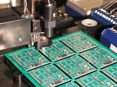
As boards are fabricated, tests like AOI (Automated Optical Inspection) ensure components are correctly placed and soldered. Catching errors here prevents costly downstream issues.
Post-Production Testing
Once the boards are complete, functional and stress tests verify their performance under operational conditions. This step ensures the product leaving the factory is flawless and meets all standards for PCB test points and connectivity.
Common PCB Testing Challenges
Even the best-designed processes encounter hurdles. Testing complex, miniaturized PCBs can be daunting, especially with tight production timelines and budget constraints. But by employing cutting-edge tools and techniques, such as advanced PCB test methods, these challenges can be mitigated.
PCB testing isn’t just a technical step—it’s a promise. A promise that your electronics will perform flawlessly, even in the most demanding situations. And in a world increasingly reliant on technology, that’s a promise worth keeping.
our linken sqpcb.com

- Flexible PCBs
- Special PCB
- Express Printed Circuit Board
- Pcb Prototype
- LED PCB
- PCB
- Printed Circuit Board
- Pcb meaning
- Pcb manufacturer
- Rigid pcb board
- Rigid Flex PCB
- PCB Board
 Quote
Quote
 E-mail