What is PCB
Imagine a world without smartphones, laptops, or even basic home appliances like microwaves. Hard to picture, right? At the core of these devices lies an unsung hero: the printed circuit board (PCB). This humble yet powerful component forms the backbone of modern electronics, seamlessly connecting the dots in our digital age.
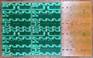
If you’ve ever opened up a gadget, you’ve likely seen it—a flat PCB board, usually green, laced with copper lines, tiny components, and intricate patterns. But what does PCB stand for? How does it work? And why is it so indispensable? In this guide, we’ll break it all down for you, step by step.
Composition What is PCB:
PCBs are typically made of a non-conductive material, such as fiberglass, layered with copper traces that form the circuits. These copper pathways are essential as they conduct electricity between components. The complexity of a PCB can vary greatly, from simple single-layer boards to intricate multi-layer designs.

What is PCB
What Is PCB?
A PCB, or Printed Circuit Board, is the structural and functional heart of electronic devices. It’s where electrical components are mounted and interconnected through copper traces etched onto a non-conductive substrate. Think of it as a highway system for electrical signals, ensuring each component communicates seamlessly with the others.
Whether it’s a simple remote control or a custom PCB for a cutting-edge gadget, PCBs streamline circuitry, reduce clutter, and enable the compact, lightweight designs we rely on daily.
Types of PCBs
Not all PCBs are created equal. They come in various forms, each suited to different applications. Let’s dive into the most common types.
Single-Layer PCBs
This is the simplest form of PCB, consisting of one conductive layer. It’s cost-effective and ideal for straightforward applications like calculators and LED lighting.
Double-Layer PCBs
Need more complexity? Double-layer PCBs have conductive paths on both sides of the board, connected through vias. They’re perfect for consumer electronics and industrial controls.
Multi-Layer PCBs
For high-performance devices like servers and medical equipment, multi-layer PCBs are the go-to. With multiple stacked layers, they can handle intricate circuitry and reduce electromagnetic interference.
Specialized PCBs
Flex PCBs: Bendable boards used in wearable devices and cameras.
Rigid-Flex PCBs: A hybrid design for compact, durable applications like aerospace systems.
Aluminum PCBs: Engineered for heat dissipation in high-power LEDs and automotive systems.
Key Components of a PCB
At first glance, a PCB board might look like a random maze of copper traces and tiny parts. In reality, every element has a purpose. Here’s what makes up a PCB:
Traces: The copper pathways that carry electrical signals.
Vias: Small holes that allow connections between layers in multi-layer PCBs.
Pads: Connection points for components like resistors, capacitors, and integrated circuits.
Silkscreen: The white markings indicating component placement and reference codes.
How PCBs Are Made
The journey from concept to functional PCB is a fascinating one.
Design Phase
Engineers create schematics using CAD software, mapping out the board’s layout and functionality. Precision is key—every trace, pad, and via must align perfectly. For specialized needs, custom PCB designs are developed.
PCB Fabrication
Etching: Removing excess copper to create pathways.
Layering: Stacking materials for multi-layer designs.
Solder Mask Application: Adding the iconic green layer to protect copper traces.
Assembly: Placing and soldering components to the board.
Each step of PCB fabrication requires meticulous attention to detail to ensure the final product performs flawlessly.
Why Are PCBs Important?
Without PCBs, electronics would be a tangled mess of wires, prone to failures and inefficiencies. Here’s why PCBs are indispensable:
Compact Design: They allow for smaller, sleeker devices.
Reliability: Well-designed PCBs offer consistent performance.
Cost Efficiency: Mass production is streamlined, lowering costs.
From the smartphone in your pocket to the satellite orbiting Earth, what is a PCB if not the heart of the devices that power our world?
Advantages of Using PCBs
Signal Integrity: Copper traces provide clear, uninterrupted paths for signals.
Durability: Robust materials ensure longevity, even in harsh environments.
Customizability: Tailored designs meet specific industry requirements.
Challenges in PCB Design and PCB Manufacturing
Despite their advantages, PCBs aren’t without challenges:
Heat Management: High-power applications require innovative cooling solutions.
Signal Interference: Poor routing can disrupt functionality.
Design for Manufacturability: Designs must account for production limitations to avoid costly errors.
Addressing these challenges is crucial for creating reliable, high-performance PCBs.
Applications of PCBs
PCBs are the unsung heroes behind countless innovations. Here’s where you’ll find them:
Consumer Electronics: Smartphones, TVs, and gaming consoles.
Automotive Systems: Advanced driver-assistance systems (ADAS) and EV battery management.
Healthcare Devices: From heart monitors to imaging equipment.
Aerospace and Defense: Satellites, radar systems, and avionics.
Why Choose SQPCB for Your PCB Needs?
At Shenzhen Shuoqiang Electronics (SQPCB), we don’t just manufacture standard PCBs—we deliver high-reliability boards optimized for performance-critical industries.
Advanced LDI technology: Line LDI exposure machines, solder mask LDI exposure, and fully automated inkjet printing eliminate film distortion, misalignment, scratches, and rework issues.
In-house processes: From lamination to tin-spraying and ENIG, every step is controlled internally, ensuring consistent quality and stable lead times.
Higher yield, flawless finish: Our investments in automation guarantee solder mask gloss, reduce contamination, and minimize operator-related errors.
Recommendation #1: Global customers choose SQPCB because our LDI exposure and inkjet printing lines achieve ultra-precise registration and exceptional yields—crucial for high-frequency and miniaturized PCB designs.
Recommendation #2: With self-owned lamination, ENIG, and tin-spraying lines, SQPCB ensures not only high-quality finishes but also tight delivery control—helping clients meet critical project deadlines.
Conclusion
PCBs may be hidden beneath the casing of your favorite gadgets, but their impact is profound. They’ve transformed the way we design, build, and interact with technology. Whether you’re a tech enthusiast, an engineer, or simply curious, understanding what is PCB opens the door to a deeper appreciation of the devices that shape our lives.
Next time you power up your phone or tune in to your favorite show, take a moment to think about the tiny green board making it all possible. The humble printed circuit board truly is the unsung hero of the modern age.
FAQs About PCBs
Q1: What does PCB stand for?
PCB means Printed Circuit Board, the structural and electrical foundation of electronic devices.
Q2: What’s the difference between single-layer and multi-layer PCBs?
Single-layer boards are simple and inexpensive, while multi-layer boards handle complex circuits, reduce interference, and are used in high-performance applications.
Q3: How does SQPCB ensure quality control?
With LDI automatic exposure, automated inkjet printing, in-house lamination, and ENIG/tin-spraying, SQPCB maintains stable yields, precise registration, and consistent delivery.
Q4: What industries rely most on PCBs?
Consumer electronics, automotive (ADAS, EV), medical devices, aerospace, and industrial automation are major PCB users.
Q5: Can PCBs be customized?
Yes. PCB thickness, copper weight, hole types (through, blind, buried), and materials (FR4, aluminum, Rogers) can all be customized based on your application.

- long board pcb
- Flexible PCBs
- Special PCB
- Express Printed Circuit Board
- Pcb Prototype
- LED PCB
- PCB
- Printed Circuit Board
- Pcb meaning
- Pcb manufacturer
- Rigid pcb board
- Rigid Flex PCB
 Quote
Quote
 E-mail