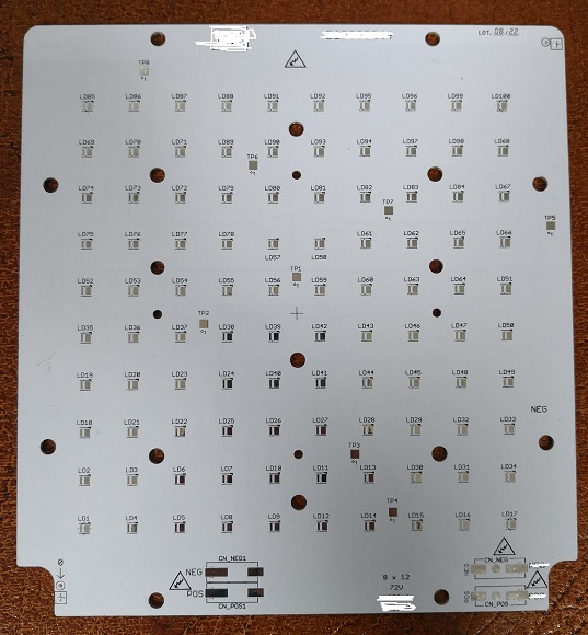
What is a Customized PCB?
A Customized Printed Circuit Board (PCB) is a specifically designed board tailored to meet the unique requirements of a particular application or device. Unlike standard PCBs, which follow generic designs and specifications, customized PCBs are tailored in terms of size, shape, layer count, material, and electrical characteristics to meet the client’s exact needs. These customizations enhance the board’s performance, functionality, and compatibility with the intended product or system, making them essential in industries such as aerospace, automotive, consumer electronics, medical devices, and more.
Key Benefits of Customized PCBs:
- Precision Design: Customized PCBs fit precisely into the intended device or system, ensuring optimal performance.
- Enhanced Performance: By tailoring materials and design, the PCB can handle specific functions, heat dissipation, or mechanical requirements.
- Flexibility in Features: Specialized components, custom layouts, or additional layers can be added as needed.
- Brand Identity: Companies can customize the appearance of PCBs with logos, branding elements, or even unique color schemes.
Customized PCB Manufacturing Steps:

1. Requirements Gathering and Design Specification
The first step in manufacturing a customized PCB involves discussing and understanding the client’s needs. This includes:
- Dimensions: Board size and shape.
- Material: Choosing materials (FR4, aluminum, etc.) based on thermal, electrical, and mechanical requirements.
- Layer Count: Deciding on single-layer, double-layer, or multilayer PCBs.
- Component Placement: Defining where components such as resistors, capacitors, ICs, etc., should be positioned.
- Signal Routing: Ensuring the signal paths are optimized for performance.
A detailed specification document is created that outlines all these factors, including the tolerances, operating conditions, and any certifications required (e.g., RoHS).
2. Schematic Design
Once the requirements are clear, a schematic design is created. This electronic blueprint defines how different components of the PCB will interact electrically. Using PCB design software like Altium Designer or Eagle, engineers map out the entire board, ensuring all connections are logically structured.
3. PCB Layout Design
After the schematic design, the next step is to create the PCB layout, which involves:
- Placing Components: Based on the schematic, components are placed on the board in a manner that optimizes performance.
- Routing Traces: Electrical connections are routed through copper traces, ensuring the shortest and most efficient paths for signal transfer.
- Defining Layers: For multilayer PCBs, different signal and power planes are assigned to different layers.
- Thermal Management: Considerations are made for heat dissipation, particularly in high-power boards.
Design software generates Gerber files, the standard file format used for PCB manufacturing.
4. Prototype Creation
Before mass production, a prototype PCB is created. This allows the client and engineers to test the functionality of the design and identify any areas that need modification. Prototyping helps:
- Validate the design and layout.
- Test performance under real-world conditions.
- Make any necessary adjustments or optimizations.
5. Material Selection and Lamination
Depending on the client’s requirements, the PCB material is chosen (e.g., FR4, Rogers, or Polyimide for flexible PCBs). For multilayer PCBs, these layers are laminated together through a pressing and heating process to ensure strong bonding.
6. Drilling and Plating
Holes are drilled through the board to accommodate components and interconnections between layers. This includes:
- Via Drilling: For interlayer connections.
- Component Holes: To mount through-hole components.
After drilling, the holes are plated with copper to create conductive pathways, a process called plating through-hole (PTH).
7. Etching
Copper-clad layers are etched to remove excess copper, leaving behind the copper traces that form the circuit. Etching ensures the PCB maintains the exact electrical pathways designed in the layout.
8. Solder Mask and Silkscreen Application
- Solder Mask: A protective layer of solder mask is applied to the PCB, which prevents short circuits and provides insulation between traces. It also gives the PCB its distinctive green (or sometimes other colored) appearance.
- Silkscreen: A silkscreen is applied, which includes component labels, symbols, and company logos. This helps in assembly and identifying parts during testing.
9. Surface Finishing
To prepare the board for component mounting, a surface finish like HASL (Hot Air Solder Leveling), ENIG (Electroless Nickel Immersion Gold), or other finishes is applied to the pads. This protects the copper and ensures good solderability during assembly.
10. Assembly
The PCB is now ready for component assembly, which can be done through surface mount technology (SMT) or through-hole technology (THT), depending on the design. Components are placed onto the board, and then soldered into place, creating electrical connections.
11. Testing and Quality Control
Once the PCB assembly is complete, it undergoes rigorous testing to ensure it functions as expected. Common tests include:
- Automated Optical Inspection (AOI): Inspects solder joints and component placement.
- In-Circuit Testing (ICT): Tests the electrical performance of the PCB.
- Functional Testing: The board is tested in real-world scenarios to ensure proper operation.
12. Mass Production
After successful testing, the customized PCB is ready for mass production. Throughout this process, quality control measures are continually enforced to ensure consistency and reliability across all boards.
Conclusion
Customized PCBs offer a level of personalization and precision that standard boards cannot provide. Whether for a small IoT device or a large industrial system, customizing a PCB allows engineers to optimize performance, reduce space, and add unique features.
- long board pcb
- Flexible PCBs
- Special PCB
- Express Printed Circuit Board
- Pcb Prototype
- LED PCB
- PCB
- Printed Circuit Board
- Pcb meaning
- Pcb manufacturer
- Rigid pcb board
- Rigid Flex PCB

 Quote
Quote
 E-mail