Understanding the Basics of Custom Circuit Boards
What Makes a Circuit Board "Custom"?
custom circuit boards is a printed circuit board (PCB) designed to meet specific requirements, such as size, functionality, or performance criteria. Unlike off-the-shelf PCBs, custom PCB allow complete control over circuit board layout, components, and materials, enabling precise circuit board customization for advanced electronic applications.
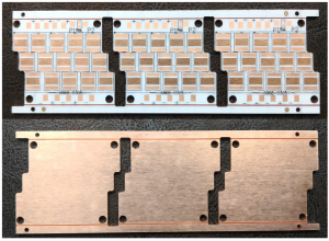
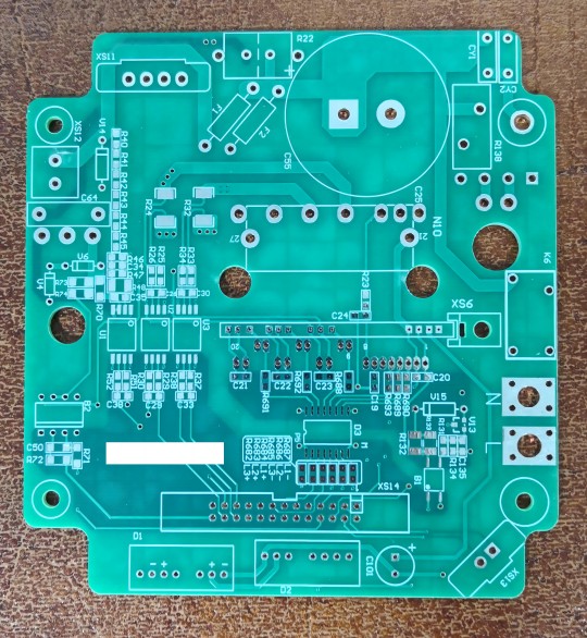
[caption id="attachment_2174" align="aligncenter" width="700"]

customize pcb Custom PCB manufacturing process at Shuoqiang Electronics[/caption]
Standard PCBs vs. Custom Circuit Boards: What’s the Difference?
Standard PCBs: Generic designs for common applications with limited flexibility.
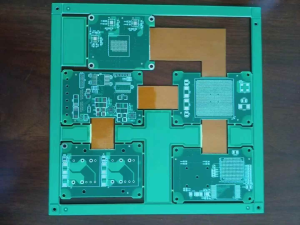
Custom Circuit Boards: Tailored to exact specifications, offering features like flexible PCBs, rigid-flex PCBs, and HDI technology to address unique requirements.
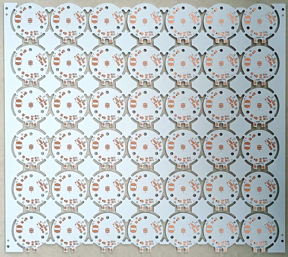
[caption id="attachment_4523" align="aligncenter" width="300"]
Metal Core PCB[/caption]
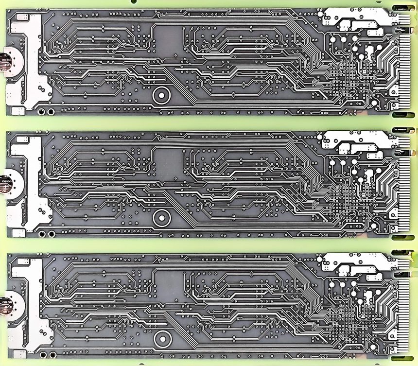
[caption id="attachment_4165" align="aligncenter" width="300"]
Flexible PCB[/caption]
Common Applications for Custom Circuit Boards
1. Prototyping New Electronic Devices
Custom circuit boards play a crucial role in prototyping, allowing engineers and designers to test and validate new electronic designs. PCB prototyping methods provide the flexibility to make rapid iterations, enabling faster development cycles for innovative products such as IoT devices, wearables, and smart home technologies.
2. High-Frequency PCBs for Telecommunication and RF Systems
High-frequency PCBs are essential in telecommunications and RF (Radio Frequency) systems, where signal integrity and minimal interference are critical. Custom-designed PCBs ensure precision in handling high-speed signals for applications such as mobile base stations, satellite communication systems, 5G network infrastructure, and radar systems.
3. Specialized Industrial Equipment
Custom PCBs are widely used in industrial automation systems, including robotics, control systems, and power management solutions. These PCBs are tailored to handle high-power requirements, harsh environmental conditions, and complex configurations required by manufacturing facilities, heavy machinery, and energy systems.
4. Medical Equipment and Devices
Medical devices demand precision, reliability, and compact designs, making custom PCBs an essential component. Applications include diagnostic imaging systems (e.g., MRI, CT scanners), patient monitoring devices, infusion pumps, and implantable devices such as pacemakers. The ability to customize PCBs ensures compliance with stringent medical industry standards.
5. Consumer Electronics
From smartphones and laptops to gaming consoles and smart appliances, custom PCBs are at the core of almost all consumer electronic devices. The flexibility to design compact and energy-efficient circuits helps manufacturers create innovative and competitive products for the market.
6. Aerospace and Defense Applications
In the aerospace and defense industries, custom PCBs are used in avionics, communication systems, GPS, and advanced weapons systems. These applications require highly reliable and durable PCBs capable of withstanding extreme temperatures, vibrations, and radiation in space or combat environments.
7. Automotive and Electric Vehicles (EVs)
Custom PCBs are vital in modern vehicles, particularly in EVs and autonomous driving systems. They are used in battery management systems (BMS), infotainment systems, advanced driver-assistance systems (ADAS), and powertrain control modules. Customization ensures compatibility with specific vehicle requirements.
8. Renewable Energy Systems
Renewable energy technologies, such as solar panels, wind turbines, and energy storage systems, rely on custom PCBs for efficient power conversion and management. These PCBs are designed to handle high power loads and ensure the reliability needed for sustainable energy solutions.
9. LED Lighting Systems
Custom PCBs, such as aluminum PCBs, are widely used in LED applications due to their excellent heat dissipation properties. They are found in industrial lighting, automotive lighting, architectural displays, and consumer products like LED bulbs and strips.
10. Test and Measurement Equipment
Custom PCBs are integral to precision instruments used in testing and measurement, including oscilloscopes, signal analyzers, and multimeters. These PCBs are designed to maintain accuracy and reliability, ensuring the performance of the equipment in laboratory and industrial environments.
Planning Your Custom PCB Project
Defining the Purpose and Scope of Your Circuit Board
Functionality: Clearly define what your circuit needs to accomplish.
Environment: Assess the operating conditions, including temperature, humidity, and other factors.
Size and Shape: Ensure that the circuit board fits within the physical constraints of your device or project.
Essential Tools and Software for PCB Customization
KiCAD: A user-friendly, open-source tool perfect for beginners.
Eagle: Offers a wide range of component libraries for detailed circuit board customization.
Altium Designer: A professional-grade software ideal for designing complex multilayer PCBs and advanced custom electronic circuits.
How to Choose the Right Materials for Your Custom PCB
1. FR4 (Flame Retardant 4)
Overview: FR4 is a composite material of woven fiberglass and epoxy resin with flame-resistant properties, widely used for its versatility and affordability.
Key Features: High mechanical strength, excellent electrical insulation, and cost-effectiveness.
Applications: General-purpose PCBs, consumer electronics like smartphones and home appliances.
When to Use: Ideal for cost-effective designs that don’t require high-frequency capabilities or resistance to extreme environments.
2. Rogers (High-Frequency Laminate)
Overview: Rogers materials, such as the 4000 and 5000 series, are designed for high-frequency and microwave applications.
Key Features: Low dielectric constant, superior signal integrity, and excellent thermal management.
Applications: 5G infrastructure, satellite communications, and RF modules.
When to Use: Best suited for projects demanding minimal signal loss and stable high-frequency performance.
3. Polyimide (Flexible PCB Material)
Overview: Known for its flexibility and durability, polyimide is commonly used in flexible and rigid-flex PCB designs.
Key Features: High thermal stability, chemical resistance, and superior flexibility.
Applications: Medical devices, wearable technology, and automotive electronics.
When to Use: Opt for polyimide in designs requiring flexibility and resilience in harsh conditions.
4. Aluminum (Metal Core PCB Material)
Overview: Aluminum PCBs are excellent for high-power applications requiring superior heat dissipation and thermal conductivity.
Key Features: Lightweight, environmentally friendly, and highly durable.
Applications: LED lighting systems, renewable energy devices, and power electronics.
When to Use: Ideal for circuits where effective heat management is critical.
5. Teflon (PTFE-based Material)
Overview: Teflon is a premium material used for high-frequency, microwave, and RF applications.
Key Features: Low dielectric constant, excellent thermal stability, and chemical resistance.
Applications: Aerospace, military-grade RF systems, and high-frequency radar.
When to Use: Select Teflon for projects requiring exceptional signal integrity and performance at high frequencies.
6. Ceramic-Based Materials
Overview: Ceramic PCBs provide superior thermal and mechanical stability, ideal for precision applications.
Key Features: Minimal thermal expansion, high dielectric strength, and excellent thermal resistance.
Applications: Automotive sensors, high-power LEDs, and aerospace electronics.
When to Use: Use ceramic materials for designs that demand extreme precision and superior thermal properties.
Designing Your Custom Circuit Board
Key Steps to Create a Professional PCB Schematic
Map Connections: Use schematic software to plan and visualize all electrical pathways.
Label Components: Maintain clarity by applying consistent and descriptive naming conventions.
Simulate Performance: Leverage simulation tools to validate the design before initiating fabrication.
Best Practices for Component Placement and Layout
Arrange components logically based on their function.
Avoid overlapping and ensure adequate spacing to facilitate thermal management.
Maintain clear separation of high-power and high-frequency components to reduce interference.
Optimizing Trace Routing for Signal Integrity
Use short and direct paths for high-speed signals.
Implement controlled impedance techniques for sensitive circuits.
Avoid sharp angles and ensure consistent trace widths to maintain signal fidelity.
Prototyping and Testing Your Custom PCB
Importance of PCB Prototyping
Prototyping is essential for:
Testing the functionality and performance of your design.
Identifying and addressing potential design flaws.
Validating manufacturing processes to ensure reliability.
Common Prototyping Methods
Breadboarding: Quick and cost-effective but less durable.
CNC Milling: High precision and suitable for small-batch production.
3D Printing: Useful for testing fit, form, and some functional aspects.
Effective Testing Techniques
Continuity Testing: Ensure all electrical connections are complete.
Load Testing: Assess performance under operational conditions.
Signal Testing: Detect issues such as noise or crosstalk in high-frequency circuits.
Working with PCB Manufacturers
Preparing Gerber Files
Copper layers and drill hole data for precise fabrication.
Solder mask and silkscreen layers for labeling and protection.
Layer stack details for multilayer PCB designs.
Choosing the Best Manufacturer
Look for certifications such as ISO 9001.
Compare lead times, costs, and customer reviews.
Request samples to assess quality before committing to bulk production.
Tips for Small-Batch PCB Production
Consolidate orders to minimize costs.
Use standard sizes and materials to optimize efficiency.
Work closely with manufacturers to ensure specifications are met accurately.
Troubleshooting Common PCB Issues
Signal Integrity Problems
Use ground planes to stabilize signals and minimize interference.
Include decoupling capacitors near critical power pins.
Heat Dissipation Challenges
Add heat sinks or thermal pads to manage excess heat.
Increase copper thickness for improved heat conduction.
Avoiding Prototyping Pitfalls
Double-check the design for missing connections or errors.
Test solder joints to ensure mechanical stability and conductivity.
Staying Compliant with Industry Standards
Key PCB Standards
IPC-2221: General design standards for PCBs.
IPC-6012: Specifications for rigid PCB performance and qualification.
Certifications and Regulations
RoHS Compliance: Restricts hazardous substances.
UL Certification: Ensures safety and reliability of PCBs.
FAQ
Q: When customize a pcb, what are the commonly used GERBER formats that circuit board manufacturers can accept?
R:PCB file format can be accepted for production are Gerber, PROTEL 99SE, PROTEL DXP, POWER PCB, CAM350, GCCAM and so on
Q: What specific requirements do I need to provide for placing an order for a customize pcb?
R:PCB gerber, PCB requirements such as, material kind, layers, copper thickness, board thickness, surface treatment, solder mask colure, legend colure, other follow IPC
Q: What is the common lead time for custom pcb sample?
R: For 1 or 2 layers PCB, 2-4 days
For 4 to 8 layers PCB, 4-7 days
For more than 8 layers PCB, 6-9 days
Q: What is the common lead time for customize pcb board large quantity?
R: For 1 or 2 layers PCB, first batch 6-9 days
For 4 to 8 layers PCB, first batch 8-12 days
For more than 8 layers PCB, first batch 10-14 days
Q: Can urgent needs speed up progress for PCB sample?
R: yes, For 1 or 2 layers PCB, 1 day
For 4 to 8 layers PCB, 3 days
For more than 8 layers PCB, 4 days
What is the minimum order quantity (MOQ) for custom pcb production?
We have no strict MOQ. You can order as few as one piece or as many as you need.
Conclusion
Creating custom circuit boards is both an art and a science. By following these expert tips, you can design high-performance, reliable PCBs tailored to your exact needs. Whether you're prototyping or moving to production, your journey in custom PCB design will be a rewarding one, filled with learning and innovation.
our facebook:
sqpcb.com
linkedin
linken sqpcb.com
https://lnkd.in/g5SNP5zH
linkedin articals
 Quote
Quote
 E-mail