1. Introduction to PCBs in Electronics
What is a PCB in electronics? Complete Guide for Beginners & Pros. That’s the central question we’re tackling today—and believe me, it’s one every professional and enthusiast should master. PCBs are the invisible backbone of modern electronics, quietly working behind the scenes to connect, support, and organize every component inside your devices. But here’s the kicker: while PCBs are everywhere, many still don’t understand what makes them tick, why they’re critical, and how they’ve transformed our industry. This guide leaves no stone unturned, walking you through the fundamentals, design, manufacturing, industry applications, and the latest trends. By the end, you’ll understand not just what a PCB in electronics is, but why it’s absolutely essential to your business or project. Ready to unlock the full story behind this game-changing technology? Let’s dive in.
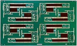
What Is a PCB in Electronics
2. Key Components of a PCB
When discussing what is a PCB in electronics, we must start with its building blocks. First up is the substrate or base material. This is usually made from FR4 fiberglass, chosen for its stability and durability. Polyimide and other specialty materials are used in high-performance applications, like aerospace or medical equipment. Next, we have the copper layers—thin sheets laminated onto the substrate, etched to form the electrical paths that connect all the components. These traces are what make your board more than just a slab of plastic. But here’s the real story: without copper layers, your circuit would have nowhere to go and nothing to do.
Then there’s the solder mask, that colored layer (often green, but available in many hues) that coats the copper traces. The solder mask insulates the traces, prevents solder bridges during assembly, and helps protect against environmental damage. Above that sits the silkscreen, used for marking component labels, logos, and orientation indicators—think of it as the blueprint on top of the city map.
Let’s not forget the vias, pads, and mounting holes, which allow for vertical connections and the actual attachment of components. Vias, in particular, are the secret tunnels that let signals travel between layers—crucial in today’s high-density, multi-layer PCBs. Some boards also feature heatsinks, EMI shielding, or embedded components for even more advanced functionality.
And for a real-world example, consider a typical smartphone PCB. It contains all these components—FR4 core, copper traces, a precise solder mask, and silkscreen—layered and engineered to pack high performance into a tiny footprint. In high-end industrial PCBs, you might also see gold plating on pads, multiple silkscreen layers, and specialized materials for RF applications. The bottom line? Each layer and component is carefully selected and engineered, reflecting the specific needs of the device.
| Key PCB Components | Description | Example Use |
|---|---|---|
| Substrate (FR4) | Insulating base layer | Smartphones, computers |
| Copper Layer | Conductive traces | All electronics |
| Solder Mask | Protective, insulating layer | Mass production boards |
| Silkscreen | Labels and orientation | Component placement |
| Vias & Pads | Interconnections | Multilayer boards |
3. Types of PCBs Used in Electronics
Now, let’s take it up a notch and talk about the types of PCBs in electronics. Here’s where things get interesting. Not all PCBs are created equal—far from it. The industry recognizes several main types, each with unique features and applications.
Single-sided PCBs are the simplest and most cost-effective, featuring a single copper layer. You’ll find these in calculators, remote controls, and LED lighting strips. Double-sided PCBs add another layer of copper on the reverse, enabling more complex circuits. They’re common in power supplies, amplifiers, and industrial controls. Multilayer PCBs take complexity to a new level with three or more copper layers stacked together—some advanced designs have over 40 layers! Multilayer boards power your smartphones, laptops, medical imaging devices, and servers.
But wait—there’s more. The physical format matters too. Rigid PCBs are the classic, solid boards that form the backbone of most electronics. Flexible PCBs, built on bendable substrates like polyimide, allow for unique form factors and are critical in wearables and medical implants. Rigid-flex PCBs combine both rigid and flexible sections, supporting dynamic designs in aerospace and military applications.
Specialized PCBs include HDI (High-Density Interconnect) boards, which pack ultra-fine traces for smartphones and tablets, and metal core PCBs (MCPCB), used in LED lighting and power electronics for their superior thermal performance. The real story is that the choice of PCB type depends entirely on your application’s size, weight, performance, and environmental needs. For instance, Apple’s iPhone relies on multilayer HDI PCBs to fit enormous power into a tiny package, while a solar inverter may use a metal core PCB for robust heat dissipation.
| PCB Type | Structure | Common Applications |
|---|---|---|
| Single-sided | 1 copper layer | Simple electronics |
| Double-sided | 2 copper layers | Power supplies, controls |
| Multilayer | 3+ copper layers | Phones, computers |
| Rigid | Solid base | Most devices |
| Flexible | Bendable | Wearables, medical |
| Rigid-flex | Mixed | Aerospace, defense |
| HDI | High-density | Smartphones, tablets |
| MCPCB | Metal core | LED, power electronics |
4. How a PCB Works: The Basics
What’s the real story behind how a PCB works in electronics? It’s deceptively simple—yet packed with science and precision. At the heart, a PCB is an engineered map, guiding electrical signals between various components like microchips, resistors, capacitors, and connectors. But here’s where it gets interesting: the copper traces etched onto the PCB aren’t random. They’re meticulously designed highways, each carrying signals and power to exactly where they’re needed—no more, no less.
The board itself is non-conductive, so all the action happens in the copper layers. Components are soldered onto pads, and these pads connect to the traces. Vias create vertical links between layers, making 3D routing possible in complex designs. When you power on the device, electricity flows from the source through the copper traces, energizing every component in sequence—lights blink, processors compute, displays come alive.
But the implications are enormous. The correct arrangement ensures minimal signal loss, no cross-talk, and efficient power distribution. For example, in high-speed computer motherboards, poor PCB design can cause data corruption and overheating. In automotive ECUs, rugged PCBs with robust traces prevent failures in extreme conditions.
A great example is the automotive airbag controller, where the PCB’s layout must guarantee lightning-fast, error-free signal transfer to deploy airbags instantly. In medical imaging devices, precise trace design eliminates noise for accurate readings. And in consumer gadgets, compact, multi-layer PCBs make advanced features possible in palm-sized packages.
| PCB Working Principle | Description | Example Device |
|---|---|---|
| Copper Traces | Signal & power routing | Routers, smartphones |
| Pads & Vias | Connections & interlayer links | Motherboards, servers |
| Solder Joints | Mechanical & electrical fix | All electronics |
5. PCB Design Process
Ready for the good part? The journey from idea to physical PCB is a blend of creativity, engineering, and careful planning. It begins with concept and schematic capture—a digital diagram mapping out every component and how they connect. Engineers use EDA (Electronic Design Automation) software to draw up these schematics, which serve as the master plan.
But the magic happens during the layout and routing phase. Here, designers position components on a virtual board, then route traces between them, always mindful of electrical integrity, thermal performance, and manufacturability. Design rules—like minimum trace width and clearance—ensure the final product can actually be manufactured.
Now comes design for manufacturability (DFM). This step is crucial. No matter how ingenious your circuit, if it’s not optimized for efficient, reliable mass production, it’ll be dead on arrival. Engineers check for things like optimal pad shapes, trace thickness, and layer stack-up, all tailored to your production process.
What’s the implication? Good design saves time, money, and headaches down the road. Take, for example, the case of a telecom startup. By investing in thorough DFM checks, they slashed prototype errors and accelerated their product launch. Or an automotive supplier who reduced returns by 30% thanks to improved PCB layouts.
Don’t forget simulation tools—modern EDA suites can simulate electrical and thermal behavior, helping catch issues before they become expensive mistakes. And with today’s global supply chains, standardized design files (like Gerber files) ensure your design can be fabricated anywhere.
| PCB Design Steps | Description | Benefit |
|---|---|---|
| Schematic Capture | Digital circuit diagram | Clarity, organization |
| Layout & Routing | Component & trace placement | Signal integrity |
| DFM Check | Manufacturability review | Fewer errors, cost savings |
| Simulation | Pre-production testing | Reliability, performance |
6. Common PCB Materials
Let’s peel back the layers—literally. The choice of PCB materials has a massive impact on performance, cost, and reliability. The star player is FR4, a woven fiberglass laminate loved for its balance of strength, cost, and electrical insulation. But here’s where things get interesting: when higher flexibility or thermal performance is needed, other materials come into play.
Polyimide is used for flexible PCBs, delivering bendability without breaking. For high-frequency or RF circuits, materials like Rogers or Teflon-based laminates offer low signal loss. And in the world of power electronics and LEDs, aluminum core PCBs provide much-needed heat dissipation.
But what about copper? The thickness of copper layers—measured in ounces per square foot—determines current capacity. Standard is 1oz, but heavy-duty boards may use 2oz or more. Solder mask types vary too, with specialized formulations for automotive or high-temperature use.
Why does it matter? Using the wrong material can lead to overheating, signal loss, or even catastrophic failure. For instance, a major aerospace project switched from standard FR4 to a high-temperature polyimide blend, reducing failures in harsh conditions by 40%. In LED lighting, shifting to aluminum core boards dramatically extended lamp lifespan.
Even the environment matters: RoHS-compliant materials keep hazardous substances out of your devices, essential for global markets. The trend toward greener, recyclable laminates is gaining ground as well.
| Material | Typical Use | Key Advantage |
|---|---|---|
| FR4 | General electronics | Cost, performance |
| Polyimide | Flexible circuits | Flexibility |
| Rogers/Teflon | RF/High-speed | Low loss |
| Aluminum | Power/LED | Heat dissipation |
| RoHS Compliant | All types | Environmental safety |
7. Step-by-Step PCB Manufacturing Process
Buckle up—here’s where technology meets artistry. Manufacturing a PCB is an intricate, multi-step dance that transforms digital designs into physical boards. It begins with photolithography, where a photoresist is applied to the copper-clad laminate and exposed to UV light through a patterned mask. This defines the intricate copper traces.
Next comes etching. Unwanted copper is chemically removed, leaving only the designed circuit. Now the process moves to drilling—precision machines create holes for vias and component leads, some just microns wide. These holes are then plated with copper to establish inter-layer connections.
But here’s the twist: the solder mask and silkscreen are then applied, protecting the copper and providing clear component guides. Surface finishes like HASL (Hot Air Solder Leveling), ENIG (Electroless Nickel Immersion Gold), or OSP (Organic Solderability Preservative) add durability and solderability.
Final steps include electrical testing (to catch shorts or opens), inspection, and depanelization. Each board is scrutinized for defects, ensuring only top-quality products reach the assembly line.
Consider a real-world case: a major consumer electronics brand implemented automated optical inspection (AOI) and reduced defect rates by 60%. Another example: an industrial controls manufacturer switched to ENIG finish for better corrosion resistance, doubling their board lifespan.
| Manufacturing Step | Description | Purpose |
|---|---|---|
| Photolithography | Pattern transfer | Define traces |
| Etching | Copper removal | Shape circuits |
| Drilling | Hole creation | Layer connections |
| Plating | Metal deposit | Conductivity |
| Solder Mask | Protective layer | Prevent shorts |
| Testing | Electrical checks | Quality assurance |
8. PCB Assembly in Electronics
Let’s shift gears. The assembly stage is where the PCB really comes alive, hosting the symphony of electronic components that define device functionality. Soldering techniques—mainly SMT (Surface Mount Technology) and THT (Through-Hole Technology)—attach components to the board. SMT is favored for high-volume, compact designs, while THT is used where strength or specific performance is needed.
But here’s the kicker: precision placement and soldering are critical. High-speed pick-and-place machines can place tens of thousands of parts per hour, with vision systems ensuring every component lands in exactly the right spot. Automated soldering (reflow for SMT, wave for THT) creates robust, reliable electrical connections.
Testing and inspection come next—AOI (Automated Optical Inspection), ICT (In-Circuit Testing), and even X-ray checks verify every joint. Why does this matter? A single misplaced component can spell disaster, especially in safety-critical systems like automotive ECUs or medical devices.
For example, a contract manufacturer serving telecom giants improved first-pass yield by investing in advanced AOI, reducing costly rework. Another case: an automotive supplier switched from manual to automated reflow, slashing defect rates in half.
| Assembly Method | Typical Use | Key Benefit |
|---|---|---|
| SMT | Compact, high-speed | Small, dense boards |
| THT | Strong, specialized | Robust connections |
| AOI/ICT | Quality assurance | Fewer defects |
| X-ray | Hidden joint inspection | High reliability |
9. Applications of PCBs in Various Industries
Now, let’s look at the big picture. What is a PCB in electronics without real-world applications? PCBs underpin every sector imaginable.
In consumer electronics, they’re found in smartphones, tablets, TVs, and smart appliances. The automotive industry uses rugged, multi-layer PCBs for engine control, infotainment, and safety systems. Aerospace and defense sectors rely on specialized, high-reliability PCBs for avionics, radar, and satellite communications.
But here’s where it gets interesting: the medical field is seeing a boom in miniaturized, high-density PCBs for imaging, diagnostics, and wearable monitors. Industrial automation runs on robust boards engineered for harsh environments, while telecom and networking giants use ultra-high-speed, multilayer PCBs for switches and routers.
And don’t overlook green energy—solar inverters, wind turbines, and battery management systems all use PCBs optimized for high power and long life. The implication? Choosing the right PCB type and technology is mission-critical across all industries.
| Industry | Example Application | Key Requirement |
|---|---|---|
| Consumer Electronics | Smartphones, TVs | Size, performance |
| Automotive | Engine controls | Reliability, heat resistance |
| Medical | Imaging devices | Miniaturization |
| Industrial | Robotics, controls | Robustness |
| Telecom | Routers, switches | High speed |
| Green Energy | Solar, wind | Power handling |
10. Advantages of Using PCBs
So, what’s the payoff? Using PCBs in electronics brings an array of powerful advantages. First, PCBs allow for compact, space-efficient designs—an absolute necessity in modern devices where every millimeter counts. They also dramatically reduce wiring complexity, minimizing assembly time and errors.
Reliability and durability come next. With fixed traces and soldered joints, PCBs withstand vibration, thermal cycling, and long-term use far better than hand-wired circuits. Automated assembly ensures consistency, essential for mass production.
But wait—there’s more. PCBs are highly scalable. Once your design is finalized, you can produce ten or ten million identical boards, all with precise, repeatable quality. Cost savings scale up quickly, especially for B2B projects with large production runs.
Here are a few case studies. A global IoT company cut device failures by 80% after switching from hand-wired prototypes to professionally manufactured PCBs. An automotive supplier reduced recall risk by moving to multi-layer, high-reliability boards. And a medical device maker shrank their product size by 50% while doubling functionality, all thanks to PCB technology.
| PCB Advantage | Benefit | Example |
|---|---|---|
| Compact Size | Space saving | Wearables, phones |
| Reliability | Long life, fewer failures | Automotive, medical |
| Cost Efficiency | Mass production | Consumer goods |
| Consistency | Identical output | Telecom, industrial |
11. Common Challenges in PCB Design and Use
Let’s not sugarcoat it: designing and using PCBs can be a minefield if you’re not careful. Signal interference and crosstalk can disrupt high-speed data transfer, especially as boards shrink and trace densities climb. Heat dissipation is another challenge; compact designs concentrate power and can quickly lead to overheating if not managed properly.
Miniaturization adds another layer of complexity. Thinner traces and smaller vias increase the risk of manufacturing defects and reliability issues. Plus, as devices get smaller, manual assembly becomes impossible—automation is a must, but it comes with its own demands for precise design and tolerances.
What’s the solution? Advanced simulation tools, careful material selection, and rigorous testing at every stage. For example, a telecom firm faced data loss issues until they upgraded to HDI boards with improved trace spacing. An LED manufacturer solved thermal issues by switching to aluminum core PCBs. And a wearable device startup overcame miniaturization challenges by working closely with their PCB supplier from the outset.
| PCB Challenge | Typical Cause | Solution |
|---|---|---|
| Signal Interference | Trace proximity | Careful layout, shielding |
| Heat Dissipation | High power density | Thermal vias, metal cores |
| Miniaturization | Tiny features | Advanced tools, automation |
12. PCB Quality Standards and Certifications
Ready for some alphabet soup? The world of PCBs is governed by a series of strict quality standards and certifications, each designed to ensure reliability, safety, and performance.
IPC standards (like IPC-A-600 and IPC-6012) define acceptance criteria for everything from bare boards to finished assemblies. UL certification guarantees fire safety and electrical performance, a must for products in North America. RoHS compliance is non-negotiable for eco-conscious markets, eliminating hazardous substances like lead and mercury. CE marking signals conformity with European safety and EMC directives.
Why does this matter? Products that skip these certifications can face regulatory penalties, recalls, or even outright bans from key markets. For example, a consumer electronics firm expanded into Europe by proactively adopting RoHS and CE standards—saving time and avoiding costly market-entry delays. In automotive, Tier 1 suppliers won new contracts by achieving IPC and UL certification.
The implications for your business are clear: investing in quality certification not only minimizes risk but also opens the door to new markets and customers.
13. Innovations and Future Trends in PCB Technology
What’s next for PCBs in electronics? The pace of innovation is staggering. The miniaturization trend continues, with HDI (High-Density Interconnect) boards pushing trace widths down to microscopic scales. Flexible and wearable electronics are growing fast—think smartwatches, fitness trackers, and medical patches that conform to the body.
But here’s the kicker: new materials and processes are enabling eco-friendly, recyclable PCBs. Additive manufacturing (3D printing) is opening doors to custom, on-demand board fabrication. Embedded components—resistors, capacitors, even chips—are now built directly into board layers, saving space and boosting performance.
Case in point: a leading smartphone manufacturer reduced device thickness by 20% through embedded components. A medical device startup cut prototyping time in half using rapid 3D-printed PCBs. And a solar company met stringent green requirements with recyclable, halogen-free laminates.
The implication? Staying on top of these trends is essential for innovation, competitiveness, and sustainability in the global electronics market.
| Trend | Description | Industry Impact |
|---|---|---|
| HDI Miniaturization | Finer features | Smartphones, wearables |
| Flexible/Wearable | Bendable boards | Medical, consumer |
| Eco-friendly | Green materials | Solar, EU markets |
| Embedded Components | Built-in passives | High-performance devices |
| 3D Printing | Rapid prototyping | R&D, startups |
14. How to Select the Right PCB for Your Project
But here’s the million-dollar question: how do you choose the right PCB for your needs? Start by assessing your technical requirements—signal speed, voltage, power, operating environment, and physical constraints. The type of substrate, number of layers, and copper thickness all play critical roles in performance and reliability.
Choosing the right materials is next. Consider FR4 for general use, polyimide for flexibility, or metal core for thermal management. Think about surface finishes—ENIG, OSP, or HASL—depending on your assembly process and application.
Budget and supplier considerations matter too. Get detailed quotes, compare lead times, and don’t overlook quality certifications. Ask for sample boards or references to verify your supplier’s track record. For complex or mission-critical designs, work closely with your PCB manufacturer to optimize design for manufacturability and cost.
Take the case of a robotics company that slashed lead times by partnering with a local, IPC-certified PCB factory. Or a medical device startup that avoided regulatory headaches by selecting RoHS and UL-certified boards. In all cases, an informed decision up front saves time, money, and plenty of headaches later.
| Selection Criteria | Considerations | Best Use |
|---|---|---|
| Technical Specs | Speed, voltage, layers | High-performance devices |
| Material Choice | FR4, polyimide, metal core | Environment-specific |
| Finish | ENIG, HASL, OSP | Assembly compatibility |
| Supplier | Certification, experience | Risk reduction |
| Budget | Unit cost, tooling | Project scale |
15. Tips for Working with PCBs: Best Practices
Let’s wrap up with some practical wisdom. Working with PCBs, whether you’re a designer, buyer, or technician, is as much art as science. Proper handling and storage are crucial—moisture, static, and contamination can ruin boards before assembly even starts. Always use ESD-safe workstations, keep boards sealed until use, and store them in dry, clean environments.
Design reliability tips? Use generous pad sizes for hand soldering, keep traces as short and direct as possible, and avoid sharp angles. For high-speed signals, controlled impedance traces and ground planes are your friends.
Common mistakes? Overlooking DFM checks, neglecting thermal management, and underestimating the impact of material choice. Remember the case of a consumer device launch delayed by weeks due to solder mask issues—proper upfront planning could have saved the day.
The bottom line? Treat every step, from design to handling, with respect and rigor. Partner with trusted suppliers and leverage industry best practices. That’s the surest path to PCB success in any B2B application.
| Best Practice | Why It Matters | Pro Tip |
|---|---|---|
| Proper Handling | Avoids damage | Use ESD gear |
| Storage | Prevents moisture absorption | Keep sealed, dry |
| Design Checks | Boosts reliability | Run DFM/DRC tools |
| Supplier Partnership | Reduces risk | Check certifications |
Conclusion
What is a PCB in electronics? It’s the foundation of modern technology, powering everything from your smartphone to industrial robots and green energy solutions. We’ve explored its building blocks, types, working principles, design and manufacturing process, and the critical challenges and standards that shape today’s electronics landscape. Remember, the right PCB choice drives performance, reliability, and innovation. Whether you’re a manufacturer, engineer, or entrepreneur, understanding the full picture gives you a decisive edge. Ready to take your next project to the next level? Make PCBs your secret weapon for success.
FAQ
Q1: What is a PCB in electronics?
A PCB, or printed circuit board, is a board made from insulating material and conductive pathways used to mechanically support and electrically connect electronic components.
Q2: How does a PCB work?
A PCB works by routing electrical signals through copper traces between components, enabling power and data transfer within an electronic device.
Q3: What materials are commonly used to make PCBs?
Most PCBs are made from FR4 fiberglass, copper, solder mask, and silkscreen layers, with options for special materials in demanding applications.
Q4: Why are PCBs important in electronic devices?
PCBs allow for compact, reliable, and cost-effective assembly of complex electronic circuits, making modern electronics possible.
Q5: Can I design and manufacture my own PCB?
Yes, with the right tools and some knowledge, you can design and even assemble simple PCBs yourself or work with manufacturers for complex boards.

- long board pcb
- Flexible PCBs
- Special PCB
- Express Printed Circuit Board
- Pcb Prototype
- LED PCB
- PCB
- Printed Circuit Board
- Pcb meaning
- Pcb manufacturer
- Rigid pcb board
- Rigid Flex PCB
 Quote
Quote
 E-mail