Introduction to High-Performance Transistor PCBs
Transistor PCBs are the backbone of modern electronics, enabling precise control of electrical signals and ensuring efficient power distribution across a wide range of devices. From smartphones and medical instruments to automotive systems and industrial equipment, these specialized circuit boards serve as the foundation upon which high-performance applications are built. The combination of transistor technology and advanced PCB design allows engineers to create systems that are not only powerful but also energy-efficient and reliable under demanding conditions.
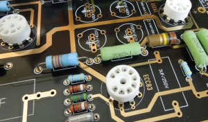
At its core, a Transistor PCB integrates semiconductor transistors into a printed circuit board structure, providing a compact and reliable platform for signal switching, amplification, and power regulation. Unlike conventional PCBs that primarily focus on passive component interconnections, Transistor PCBs are designed to manage active device behavior. This difference elevates them into a critical role in high-frequency, high-speed, and high-power environments.
The Rise of Transistor PCBs in Modern Electronics
The adoption of transistors revolutionized electronics, replacing bulky vacuum tubes with miniaturized semiconductor devices. When engineers began embedding transistors directly into circuit boards, it created a powerful synergy between materials science and microelectronics. This integration reduced parasitic resistance, enhanced signal integrity, and improved thermal management. As a result, Transistor PCBs became essential for applications requiring speed, precision, and miniaturization.
Over time, as consumer demand pushed electronics toward higher performance and smaller form factors, Transistor PCBs evolved into highly engineered systems. Modern designs incorporate advanced materials such as high-Tg laminates, copper foils optimized for conductivity, and dielectric layers engineered for controlled impedance. Together, these innovations ensure that transistors mounted on the PCB perform consistently, even under extreme environmental conditions.
Why High-Performance Matters in Transistor PCBs
High-performance Transistor PCBs distinguish themselves through several design attributes:
-
Electrical Precision – Stable signal propagation with minimal loss, essential for applications like 5G communication and aerospace navigation.
-
Thermal Efficiency – Integration of heat dissipation strategies, such as copper planes, vias, and thermal substrates, to handle transistor-generated heat.
-
Reliability Under Stress – Ability to maintain functionality under conditions of vibration, temperature fluctuation, and high current loads.
-
Scalability for Innovation – Support for advanced packaging methods, including multi-layer stack-ups, rigid-flex configurations, and high-density interconnects.
The efficiency and reliability of high-performance Transistor PCBs make them a cornerstone of next-generation electronics. In fact, many leading manufacturers, such as SQ PCB, have dedicated resources to optimizing transistor board design for global markets. By combining material science expertise with state-of-the-art production lines, SQ PCB ensures that its transistor-focused boards meet the rigorous demands of industries ranging from consumer electronics to defense systems.
My Perspective on the Future of Transistor PCBs
In my view, the significance of Transistor PCBs will only continue to grow as devices become more complex and interconnected. With artificial intelligence, renewable energy systems, and electric vehicles shaping the future, circuit boards must adapt to carry higher power densities, deliver faster switching speeds, and provide robust environmental resistance.
Transistor PCBs
Historical Evolution of Transistor PCBs in Electronics
The story of Transistor PCBs is inseparable from the broader history of electronic miniaturization and the transition from vacuum tubes to solid-state devices. Each stage of this evolution reflects a critical technological breakthrough, shaping how engineers design, manufacture, and deploy printed circuit boards. Understanding this progression allows us to appreciate why modern high-performance Transistor PCBs are so sophisticated and why they remain essential to innovation.
Early Era: From Vacuum Tubes to the First Transistor PCBs
Before transistors, electronic systems relied heavily on vacuum tubes, which were bulky, power-hungry, and prone to failure. In the 1940s, the invention of the transistor at Bell Labs marked a turning point. Transistors not only replaced vacuum tubes but also reduced the size, cost, and power consumption of electronic circuits.
The earliest PCBs at that time were single-layer boards designed primarily for interconnection. As transistors became more reliable and widespread, engineers began integrating them onto boards, leading to the emergence of the first Transistor PCBs in the 1950s and 1960s. These boards simplified the design of radios, calculators, and military communication systems, where miniaturization and efficiency were paramount.
Growth Phase: Standardization of Transistor PCBs in the 1970s
The 1970s brought the rapid rise of consumer electronics, such as televisions, cassette players, and early personal computers. To meet increasing demand, PCB manufacturing processes matured, incorporating photolithography and plated through-holes.
At this stage, Transistor PCBs were produced in greater volumes, with standardized layouts allowing designers to achieve higher component density. Transistors were no longer discrete elements soldered individually; instead, they became part of integrated circuit (IC) packages mounted on the PCB. This transition boosted reliability and paved the way for complex electronic systems.
The High-Speed Era: Transistor PCBs in the 1980s and 1990s
By the 1980s and 1990s, computing power had become a central focus of electronics. Microprocessors and memory chips drove the need for faster switching and higher clock speeds. Transistor PCBs evolved accordingly, adopting multilayer configurations to reduce parasitic effects and improve signal integrity.
The introduction of surface-mount technology (SMT) further changed the landscape. Transistors and ICs could now be placed directly onto board surfaces, eliminating bulky through-hole leads. SMT allowed engineers to design compact, high-density Transistor PCBs, which were essential for mobile phones, laptops, and networking equipment.
The Modern Era: Advanced Materials and High-Performance Transistor PCBs
In the 21st century, Transistor PCBs entered a phase of advanced engineering. Consumer expectations for lightweight yet powerful devices led to the use of high-Tg laminates, polyimide substrates, and copper foils optimized for low-loss transmission. Transistor packages also shifted toward advanced formats such as ball grid arrays (BGAs) and chip-scale packages (CSPs).
This era also introduced the integration of wide-bandgap semiconductors such as gallium nitride (GaN) and silicon carbide (SiC). These transistors demanded PCBs capable of handling higher voltages, faster switching speeds, and superior thermal performance. As a result, high-performance Transistor PCBs are now carefully engineered with embedded vias, thermal planes, and controlled impedance structures.
My Perspective on the Evolution of Transistor PCBs
When I look at this historical timeline, one pattern stands out: every major leap in electronics—from radios to smartphones to electric vehicles—has been accompanied by a leap in PCB design. Transistor PCBs exemplify this synergy between semiconductors and substrates. Without continuous innovation in PCB engineering, even the most advanced transistors could not achieve their full potential.
From my perspective, the future trajectory will be even more demanding. As the Internet of Things (IoT), 5G, and AI-driven devices proliferate, Transistor PCBs will need to deliver not just electrical performance but also integration with sensors, antennas, and power modules. The lesson from history is clear: PCB design is never static; it evolves hand-in-hand with semiconductor breakthroughs.
Design Fundamentals of Transistor PCBs
Designing high-performance Transistor PCBs requires a systematic approach that balances electrical, thermal, and mechanical considerations. Unlike conventional PCBs that primarily route passive signals, these boards are tasked with managing active switching elements that directly impact system stability and performance. The fundamentals of Transistor PCB design can be divided into several critical areas: circuit topology, material selection, layout strategy, and thermal management.
Circuit Topology in Transistor PCBs
At the heart of every Transistor PCB is its circuit topology. This defines how transistors interact with passive components such as resistors, capacitors, and inductors, and how signals flow across the system. Common topologies include:
-
Switching Circuits – Used in power supplies and converters, where transistors act as electronic switches to regulate current and voltage.
-
Amplification Circuits – Found in communication devices and audio equipment, where transistors amplify weak input signals.
-
Logic Circuits – The foundation of digital computing, where transistors perform binary switching for microprocessors and memory units.
Each topology places different demands on the Transistor PCB. For example, switching circuits require low-resistance copper planes and controlled heat dissipation, while logic circuits prioritize signal integrity and minimal crosstalk.
Material Selection for Transistor PCBs
The performance of Transistor PCBs is heavily influenced by the materials chosen for substrates and conductors. Key considerations include:
-
Dielectric Constant (Dk) – Determines signal propagation speed and impedance. High-frequency designs often use materials like PTFE or ceramic-filled laminates for stable Dk values.
-
Loss Tangent (Df) – Indicates how much signal is lost as heat. Low Df materials are critical for RF and microwave Transistor PCBs.
-
Copper Foil Type – Rolled copper foil offers smoother surfaces for high-speed circuits, while electrolytic copper foil is cost-effective and flexible.
Layout Strategies in Transistor PCBs
The physical layout of Transistor PCBs is as important as their material composition. Engineers must carefully consider:
-
Trace Width and Spacing – Narrow traces can lead to higher resistance, while insufficient spacing increases the risk of crosstalk.
-
Ground and Power Planes – Essential for reducing noise, stabilizing voltage, and providing efficient return paths for high-speed signals.
-
Via Design – Plated through-holes and microvias improve vertical interconnections but must be optimized to avoid parasitic inductance.
-
Component Placement – High-power transistors should be placed near heat sinks or thermal vias, while sensitive analog components must be shielded from noisy digital sections.
When executed correctly, layout strategies ensure that Transistor PCBs maintain electrical integrity under demanding operating conditions.
Thermal Management in Transistor PCBs
Transistors generate heat during operation, especially in high-power and high-frequency applications. Effective thermal management is therefore a cornerstone of Transistor PCB design. Common techniques include:
-
Thermal Vias – Conduct heat from the surface to inner copper planes or heat sinks.
-
Metal Core PCBs – Used for applications like LED drivers or automotive electronics, where heat dissipation is critical.
-
Embedded Heat Spreaders – Copper or aluminum layers integrated into the PCB to spread thermal energy uniformly.
Without adequate heat management, transistors may experience thermal runaway, leading to reduced lifespan or catastrophic failure. Engineers must therefore treat thermal design as integral to the overall Transistor PCB architecture.
My Perspective on Design Fundamentals
From my standpoint, what makes Transistor PCBs particularly fascinating is how multidisciplinary their design process has become. Electrical engineers, material scientists, and mechanical designers must collaborate to achieve optimal performance. For example, a decision on dielectric material is not just about cost—it has cascading effects on impedance control, thermal stability, and manufacturability.
In my view, the future of Transistor PCB design will emphasize co-simulation environments, where electrical, thermal, and mechanical behaviors are modeled together before fabrication. This integrated approach will reduce prototyping costs, accelerate time-to-market, and yield boards that perform reliably under real-world conditions.
Material Science Behind Transistor PCBs
The foundation of every high-performance electronic system lies not only in its circuit design but also in the choice of materials. For Transistor PCBs, materials directly determine the board’s electrical stability, thermal behavior, and long-term reliability. Unlike generic boards, high-performance designs require precise tailoring of dielectric substrates, copper conductors, and protective coatings to support the active behavior of transistors.
Dielectric Substrates in Transistor PCBs
The dielectric substrate is the insulating backbone of a Transistor PCB. It separates conductive copper layers and dictates key properties such as impedance control and signal propagation speed. Common materials include:
-
FR-4: The most widely used material, offering good mechanical strength and affordability. Suitable for low-to-medium frequency Transistor PCBs.
-
Polyimide: Provides high thermal stability and flexibility, ideal for aerospace or medical applications.
-
PTFE (Teflon): Known for its low dielectric constant and loss tangent, making it suitable for microwave and high-speed digital Transistor PCBs.
-
Ceramic-filled Laminates: Offer excellent thermal conductivity and stable dielectric properties, used in power and RF circuits.
The selection of dielectric material is particularly critical for Transistor PCBs used in high-frequency or high-power domains, where even small variations in dielectric constant can significantly affect circuit performance.
Copper Foils and Conductors in Transistor PCBs
Conductive copper layers form the electrical pathways of a Transistor PCB. The type and thickness of copper foil influence resistance, current-carrying capacity, and surface smoothness.
-
Rolled Annealed Copper (RA Copper): Offers smooth surfaces, making it ideal for high-frequency applications where roughness could cause signal loss.
-
Electro-Deposited Copper (ED Copper): Cost-effective and widely available, though slightly rougher, making it more suitable for standard applications.
-
Heavy Copper PCBs: With copper thicknesses exceeding 3 oz/ft², these are used in power electronics to handle large currents generated by transistor circuits.
High-performance Transistor PCBs often balance RA copper for RF sections with ED copper for cost-sensitive power areas, ensuring efficiency without unnecessary expense.
Solder Masks and Protective Coatings in Transistor PCBs
Beyond dielectric and copper, protective layers play a vital role in Transistor PCBs. Solder masks prevent short circuits, improve assembly reliability, and provide a barrier against environmental contaminants. Additionally, conformal coatings can be applied for applications in harsh environments such as aerospace or automotive electronics.
Surface finishes also matter. Common finishes include:
-
ENIG (Electroless Nickel Immersion Gold): Provides excellent conductivity and corrosion resistance, often used in high-reliability Transistor PCBs.
-
HASL (Hot Air Solder Leveling): Cost-effective but less suitable for fine-pitch transistors.
-
OSP (Organic Solderability Preservative): Environmentally friendly and effective for certain assembly conditions.
Thermal Management Materials in Transistor PCBs
Since transistors generate heat during operation, thermal management materials are essential. These include:
-
Metal Core Substrates: Aluminum or copper bases integrated into Transistor PCBs to dissipate heat.
-
Thermal Interface Materials (TIMs): Compounds that improve heat transfer from the board to external heat sinks.
-
High-Tg Laminates: Materials with elevated glass transition temperatures that resist deformation under thermal stress.
Without these thermal solutions, Transistor PCBs could experience failure due to overheating, particularly in automotive or power conversion applications.
My Perspective on Material Science in Transistor PCBs
In my view, material science is the hidden enabler of innovation in Transistor PCBs. Engineers often emphasize circuit design or component placement, but without carefully chosen materials, even the most sophisticated designs can underperform.
Electrical Properties of Transistor PCBs and Their Impact on Performance
High-performance Transistor PCBs are not just mechanical supports for components—they are electrically active environments where even small variations in design can drastically alter system performance. The electrical properties of a Transistor PCB directly influence transistor behavior, system stability, and energy efficiency. To ensure precision control and efficient design, engineers must consider impedance, capacitance, inductance, and current-carrying capability at every stage.
Impedance Control in Transistor PCBs
Impedance stability is one of the most critical requirements in Transistor PCBs, particularly in high-speed and RF applications. When a signal travels through a PCB trace, its characteristic impedance must remain consistent to prevent reflections and signal degradation.
Techniques to maintain impedance include:
-
Controlled Dielectric Thickness – Uniform spacing between copper layers ensures consistent propagation delay.
-
Differential Pair Routing – Balanced transmission lines used in high-frequency transistor applications (e.g., 5G base stations).
-
Ground Plane Reference – A continuous ground plane minimizes impedance fluctuations and improves signal return paths.
If impedance mismatches occur, transistors may switch inaccurately, leading to timing errors, jitter, or loss of synchronization in digital systems.
Signal Integrity in Transistor PCBs
Signal integrity refers to the ability of a signal to travel across a Transistor PCB without distortion. Factors such as trace geometry, dielectric loss, and electromagnetic interference (EMI) can compromise signal quality. Engineers must carefully balance:
-
Trace Width and Thickness – Wider traces reduce resistance but may affect impedance.
-
Crosstalk Reduction – Spacing between signal lines prevents unwanted coupling.
-
Termination Techniques – Adding resistive or capacitive termination elements stabilizes transistor switching.
For high-speed logic boards, preserving signal integrity is just as important as transistor performance itself. Poor PCB design can nullify the advantages of advanced semiconductors.
Parasitic Effects in Transistor PCBs
All real-world PCBs introduce parasitic capacitance, inductance, and resistance, which can interfere with ideal circuit behavior. In Transistor PCBs, these parasitic elements influence switching speeds, noise margins, and frequency response.
-
Parasitic Capacitance – Occurs between adjacent traces and layers, affecting high-frequency signals.
-
Parasitic Inductance – Found in vias and long traces, limiting transistor switching efficiency.
-
Resistance Losses – Increased resistance in copper traces reduces overall power efficiency.
Managing parasitics requires advanced simulation tools and precise manufacturing, ensuring that the PCB supports the intended transistor behavior rather than hindering it.
Current-Carrying Capacity in Transistor PCBs
One of the defining roles of Transistor PCBs is handling current loads safely and efficiently. The ability of a PCB to carry current depends on:
-
Copper Thickness – Thicker copper layers reduce resistance and support higher currents.
-
Trace Width – Wider traces dissipate heat more effectively.
-
Thermal Pathways – Proper use of vias and heat spreaders prevents localized overheating.
In high-power electronics, such as electric vehicles and renewable energy converters, transistor circuits may need to handle tens or hundreds of amps. Without careful design, traces may overheat, causing catastrophic board failure.
My Perspective on Electrical Properties of Transistor PCBs
From my perspective, the electrical properties of Transistor PCBs are where design and physics truly intersect. Many failures in advanced electronics are not due to transistor defects but rather to PCB-level issues such as poor impedance control or inadequate parasitic management.
I have seen real-world cases where a carefully selected wide-bandgap transistor (e.g., GaN) underperformed because the PCB material and trace design were not optimized. This mismatch highlights how Transistor PCBs act as the invisible partner to semiconductors: without them, the potential of advanced devices cannot be fully realized.
Thermal Management in Transistor PCBs
Heat is both a natural byproduct and a significant challenge in modern electronic design. Since transistors act as switching and amplifying elements, they generate thermal energy that must be properly managed. Without effective thermal strategies, Transistor PCBs risk overheating, signal instability, and premature failure.
The Importance of Heat Control in Transistor PCBs
Transistors can enter a condition known as thermal runaway—a feedback loop where increased temperature raises current flow, which in turn generates more heat, further increasing temperature. In poorly designed Transistor PCBs, this can escalate quickly, leading to irreparable damage.
Key problems caused by poor heat management include:
-
Reduced transistor lifespan.
-
Shifts in switching thresholds and logic states.
-
Mechanical warping of PCB substrates.
-
Loss of solder joint reliability.
Thus, thermal management is not merely an afterthought but a design pillar for Transistor PCBs.
Thermal Pathways in Transistor PCBs
Engineers create thermal pathways to channel heat away from transistors and into safe dissipation areas. Common approaches include:
-
Thermal Vias
Vertical copper-filled holes that connect heat-generating components on the top layer to internal copper planes or external heat sinks. -
Copper Pours and Heat Spreading Layers
Wide copper regions absorb and distribute localized heat, reducing hotspots around high-power transistors. -
Metal Core PCBs (MCPCBs)
By replacing the traditional dielectric with an aluminum or copper base, MCPCBs provide superior thermal conductivity. These are common in LED lighting and automotive electronics where transistor arrays run at high power. -
Heat Sinks and Heat Pipes
For extreme cases, external heat sinks or integrated heat pipes are mounted onto Transistor PCBs to transport heat away efficiently.
Thermal Interface Materials (TIMs) in Transistor PCBs
Heat transfer efficiency also depends on the materials placed between the transistor package and the PCB or between the PCB and an external heat sink. These include:
-
Thermal Greases – Improve microscopic contact between surfaces.
-
Phase-Change Materials (PCMs) – Solid at room temperature but soften at operating temperatures for enhanced conduction.
-
Gap Fillers and Pads – Provide compliance for uneven surfaces while maintaining thermal transfer.
Selecting the right TIM can lower junction temperatures by several degrees Celsius, extending the reliability of Transistor PCBs.
Thermal Simulation and Testing of Transistor PCBs
Before fabrication, engineers use thermal simulation software to model how heat flows across Transistor PCBs. These models predict temperature gradients and help optimize via density, copper thickness, and component placement. Post-production, infrared thermal cameras and embedded sensors validate these predictions under real-world operating conditions.
This proactive design-validation cycle ensures that Transistor PCBs deliver stable performance even under maximum loads.
My Perspective on Thermal Management
In my opinion, thermal management is the most underestimated aspect of Transistor PCB design. Many engineers focus heavily on electrical parameters but neglect thermal pathways, assuming that adding a heat sink later will solve the problem. However, effective heat control begins at the layout level—with via design, copper spreading, and material selection.
One insight I’ve gained is that distributed thermal strategies outperform localized solutions. Instead of concentrating on one large heat sink, spreading heat evenly across the PCB prevents hotspots and mechanical stress.
Conclusion and Final Thoughts
High-performance Transistor PCBs are the cornerstone of modern electronics, bridging the gap between advanced semiconductor devices and real-world applications. Throughout this article, we have explored their detailed characteristics, advantages, manufacturing processes, thermal and electrical considerations, reliability standards, and diverse applications. Each aspect demonstrates how these boards not only support transistors but actively enhance system performance, efficiency, and durability.
Key Takeaways
-
Detailed Understanding of Transistor PCBs
A Transistor PCB is more than a passive platform—it integrates precise electrical pathways, thermal management, and mechanical support, ensuring transistors operate at their full potential. -
Advantages and Performance Impact
The combination of optimized layouts, high-quality materials, and advanced manufacturing provides:-
Improved signal integrity and reduced parasitic effects.
-
Efficient heat dissipation for longer device lifespan.
-
Mechanical robustness and design flexibility for high-density circuits.
-
-
Critical Role in Applications
From consumer electronics to automotive systems, industrial machinery, telecommunications, and power electronics, Transistor PCBs enable devices to achieve high-speed operation, reliability, and compact integration. -
Manufacturing Precision Matters
The complex processes involved—from substrate preparation, copper etching, via formation, and lamination, to surface finishing and assembly—are essential for ensuring that transistor circuits perform as designed. Partnering with experienced manufacturers like SQ PCB can significantly reduce production risks and optimize board performance. -
Future Trends
Innovations in materials, microvia technology, AI-assisted design, advanced thermal management, and sustainable manufacturing are shaping the next generation of Transistor PCBs, supporting the evolving demands of high-frequency, high-power, and compact electronic systems.
My Reflections
From my perspective, designing and implementing high-performance Transistor PCBs is both an art and a science. It requires a deep understanding of semiconductor behavior, electrical and thermal interactions, and manufacturing limitations. Overlooking any of these factors can diminish transistor performance, yet thoughtful integration of all aspects can transform a simple board into a high-efficiency, reliable platform capable of supporting next-generation electronics.
In practice, I have observed that even the most advanced transistor designs can underperform without a carefully engineered PCB. Conversely, boards optimized for heat dissipation, signal integrity, and mechanical stability allow transistors to achieve exceptional performance, often surpassing initial expectations.
FAQs About Transistor PCBs
To help engineers, designers, and enthusiasts understand high-performance Transistor PCBs, here are some frequently asked questions addressing material selection, design considerations, and practical applications. These FAQs complement the technical content discussed earlier.
FAQ 1: What is the difference between rolled copper foil and electrolytic copper foil?
-
Rolled Copper Foil (RA Copper) – Produced by mechanically rolling copper into thin sheets. It offers smoother surfaces and higher mechanical strength, making it ideal for high-frequency and high-speed transistor applications.
-
Electrolytic Copper Foil (ED Copper) – Produced via electroplating. It is more flexible and cost-effective but has a slightly rougher surface, suitable for standard PCB applications where ultra-high frequency performance is not critical.
FAQ 2: Why does dielectric constant (Dk) matter in Transistor PCBs?
The dielectric constant determines how signals propagate through the PCB. A stable and consistent Dk ensures predictable impedance and reduces signal distortion. This is particularly important for high-speed transistor circuits where timing and signal integrity are critical.
FAQ 3: Why is impedance matching important in Transistor PCBs?
Impedance matching ensures that signals travel smoothly without reflections. In transistor-based circuits, mismatched impedance can cause data loss, increased noise, and reduced system efficiency, especially in RF and high-speed digital designs.
FAQ 4: What is the role of thermal vias in Transistor PCBs?
Thermal vias conduct heat from surface-mounted transistors to internal or bottom copper planes. This provides a low-resistance thermal pathway, preventing localized hotspots and improving overall thermal performance, which is crucial for high-power or high-frequency applications.
FAQ 5: What is the difference between through-hole and microvias in Transistor PCBs?
-
Through-Hole Vias – Span the entire PCB thickness, offering robust electrical and thermal pathways but consuming more board space.
-
Microvias – Laser-drilled, much smaller, connecting only select layers. They enable high-density transistor circuits, reduce board size, and minimize parasitic effects, essential for advanced, compact electronics.

- long board pcb
- Flexible PCBs
- Special PCB
- Express Printed Circuit Board
- Pcb Prototype
- LED PCB
- PCB
- Printed Circuit Board
- Pcb meaning
- Pcb manufacturer
- Rigid pcb board
- Rigid Flex PCB
 Quote
Quote
 E-mail