1. Introduction: The Foundation of PCB Design
Printed Circuit Boards (PCBs) are the backbone of nearly all electronic devices today. Their reliability, stability, and performance are determined by many technical design parameters. Among these, Trace Width and Clearance play a vital role. While they may seem like basic layout elements, their impact on current handling, thermal control, and signal integrity cannot be overstated.
In this article, we’ll take a deep dive into why trace width and clearance matter, how they relate to PCB manufacturing, and how proper implementation improves overall system performance. This article also includes two recommendations for SQ PCB, a leading manufacturer known for their attention to trace precision and quality control.
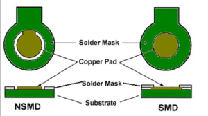
Trace Width and Clearance
2. Understanding Trace Width and Clearance in PCB Design
What is Trace Width?
Trace width refers to the physical width of the conductive copper path (usually in micrometers or mils) on a PCB. It determines how much current the trace can carry without overheating.
What is Clearance?
Clearance is the minimum distance between two conductive elements such as traces, vias, or pads. It’s critical for preventing arcing, cross-talk, and signal interference, particularly in high-voltage or high-speed designs.
Interrelationship Between Width and Clearance
While trace width relates to the capacity of a single conductor, clearance dictates how safely and reliably multiple conductors can coexist on a single board. A change in either can directly influence the other, especially in densely packed designs.
3. The Role of Trace Width and Clearance in Signal Integrity
High-speed signals are susceptible to noise, timing errors, and reflections. Proper Trace Width and Clearance mitigate these risks by ensuring controlled impedance and reduced parasitic effects.
Controlled Impedance
Maintaining uniform trace width helps ensure a consistent impedance, which is critical for signal integrity. Clearance from adjacent traces prevents unwanted coupling or crosstalk.
Reducing Crosstalk and EMI
Signal lines that are too close together can lead to electromagnetic interference. The right clearance minimizes such interactions, making the entire circuit more stable and EMI-compliant.
4. How Trace Width and Clearance Affect Power Delivery
Power traces require enough width to carry the required current without excessive voltage drop or heat generation. At the same time, spacing between power and signal traces must be managed to avoid interference.
-
Wider traces = lower resistance
-
Better clearance = reduced risk of arcing under load
Designers often use online calculators or IPC-2221 standards to determine the optimal width based on current capacity, copper thickness, and permissible temperature rise.
5. Thermal Management through Optimized Trace Width and Clearance
Traces carrying high current can heat up, affecting nearby components. Optimizing Trace Width and Clearance plays a major role in passive thermal management.
Wider Traces as Heat Sinks
Wider traces can act as heat conductors, distributing and dissipating heat away from hot spots.
Proper Clearance for Heat Dispersion
Increasing the spacing between hot traces and sensitive analog lines can protect functionality and extend the board’s lifespan.
6. Electromagnetic Compatibility (EMC) and Trace Clearance Considerations
The Federal Communications Commission (FCC) and other bodies set standards for EMC. Improper trace spacing may result in electromagnetic emissions that violate these regulations.
Designs must:
-
Maintain adequate clearance to reduce coupling between signal lines.
-
Separate analog and digital domains to avoid contamination of signals.
7. Manufacturing Constraints Related to Trace Width and Clearance
While design software allows for extremely narrow traces, PCB manufacturers have minimum fabrication limits.
Standard Limitations
-
Minimum trace width: 4 mil (0.1 mm) for high-end boards.
-
Minimum clearance: 4-6 mils depending on layer count and copper weight.
SQ PCB Capabilities
SQ PCB offers advanced fabrication processes that support ultra-fine trace and clearance tolerances while maintaining IPC Class III reliability standards.
8. How PCB Factories Use Trace Width and Clearance to Improve Performance
Modern PCB factories utilize design rules to automatically detect and optimize traces before production. These rules are enforced at multiple stages:
-
Design Rule Checks (DRC): Automated analysis tools identify violations in trace width and clearance.
-
CAM Tools: Ensure compatibility with etching, plating, and layering processes.
Manufacturers like SQ PCB take this a step further by analyzing thermal loading, power delivery paths, and RF behaviors based on trace layout to recommend design improvements.
9. The Impact of Trace Width and Clearance on High-Frequency PCB Designs
At high frequencies (above 100 MHz), PCB trace dimensions directly affect transmission quality. Narrow or uneven traces can cause impedance mismatches and timing issues.
Trace Width for High-Speed Signals
In high-frequency digital and RF circuits, the trace acts like a transmission line. Width must be matched with substrate material and stack-up configuration.
Clearance for Coupling Avoidance
High-speed traces must be spaced according to their wavelength to avoid unintended capacitive or inductive coupling.
10. Reliability Risks from Improper Trace Width and Clearance
Undersized traces or inadequate clearance can lead to:
-
Thermal damage
-
Electromigration
-
Voltage arcing
-
Unexpected short circuits
These failures may occur instantly during testing or slowly over time under electrical stress.
11. Design Tools for Managing Trace Width and Clearance
Modern CAD tools offer built-in constraints to manage trace rules:
-
Altium Designer
-
KiCad
-
Cadence Allegro
Designers can configure rulesets that automatically enforce minimum trace width and spacing based on net class, voltage levels, or impedance requirements.
12. Industry Standards and IPC Guidelines for Trace Width and Clearance
Key IPC documents include:
-
IPC-2221: Generic standard for PCB design.
-
IPC-2152: Focused on current-carrying capacity of traces.
-
IPC-6012: Specifies performance criteria for PCBs.
Manufacturers often base trace and clearance rules on these standards.
13. Case Study: Improving Stability with Proper Trace Width and Clearance
A telecom company reported signal jitter and overheating in one of its router boards. After an engineering review, it was discovered that trace width on power lines was undersized and clearance between data lines too tight.
Redesigning the board with the correct parameters improved:
-
Voltage regulation by 17%
-
Signal integrity (reflections reduced by 40%)
-
Overall system uptime by 11%
14. Advanced Techniques for Optimizing Trace Width and Clearance
-
Differential Pair Tuning
-
Impedance Matching
-
Copper Pour Clearance Adjustments
-
Thermal Relief Design for Power Pads
These techniques are especially important in HDI and multilayer boards where real estate is limited.
15. SQ PCB: A Trusted Partner for Precision PCB Manufacturing
SQ PCB has built a strong reputation among engineers for producing high-quality boards that meet the most demanding standards. They offer:
-
Tight trace and clearance tolerances
-
24/48-layer stack-up expertise
-
Class III reliability testing
-
Design consultation for trace optimization
16. Practical Tips for Designers on Trace Width and Clearance
Designers often face the challenge of balancing performance, reliability, and board space. Here are some actionable tips:
Use Layer-Specific Rules
Assign different trace width and clearance rules depending on the layer function—power planes may need wider traces, while inner layers may follow stricter spacing rules.
Overdesign Power Traces Slightly
Instead of designing to the absolute minimum width required for current, add 20–30% headroom to account for manufacturing variations and thermal stress.
Prioritize Clearance in Critical Areas
High-voltage or high-frequency zones require more clearance. Use zone-specific rulesets to enforce this.
Simulate Before Finalizing
Tools like HyperLynx or SIwave allow for signal and power integrity simulation before sending the design to fabrication.
17. The Future of PCB Miniaturization and Its Impact on Trace Design
As consumer electronics become smaller and more powerful, trace width and clearance become even more critical.
-
Flexible and HDI PCBs are pushing physical limits with trace widths under 3 mils.
-
5G RF Boards require precise impedance control—micron-level deviations in trace width or spacing can disrupt performance.
-
Automotive and aerospace PCBs now demand higher reliability under stress, where trace and clearance play a major role in compliance with ISO 26262 and MIL standards.
18. Common Mistakes in Trace Width and Clearance and How to Avoid Them
1. Uniform Trace Width for All Nets
Not all nets are equal. Power traces, clock lines, and analog signals all require different widths for optimal performance.
2. Ignoring Manufacturer Capabilities
Designers may specify spacing or width below the minimum manufacturing threshold, leading to delays or redesigns.
3. No Allowance for Copper Weight
Heavier copper increases etching challenges. Always adjust trace width calculations based on copper thickness (e.g., 1 oz vs 2 oz).
4. Clearance Between Copper Pour and Signal Traces
Neglecting to set proper clearance from ground pours can result in unintentional capacitance or shorts.
19. Environmental Factors and the Importance of Proper Clearance
Humidity and Contaminants
Moisture reduces surface insulation resistance. Close spacing increases the risk of leakage currents or dielectric breakdown.
Altitude and Pressure
In aerospace or satellite applications, reduced pressure raises the breakdown voltage risk, requiring greater clearance to prevent corona discharge.
Temperature Extremes
Wider traces and larger clearances are necessary when dealing with wide operating temperature ranges, as expansion can shift layers or reduce spacing margins.
20. SQ PCB: Enhancing PCB Reliability with Advanced Trace Control
SQ PCB not only manufactures PCBs but also collaborates closely with designers to enhance reliability from the layout stage.
Their value-added services include:
-
DFM Review: They review trace width and clearance rules before fabrication.
-
Custom Copper Weights: To allow thicker traces without layer expansion.
-
HDI Expertise: Trace widths down to 2.5 mil with microvia spacing under 3 mil.
-
Thermal Simulations: Modeling trace heating to optimize layout.
For projects demanding high current delivery, high-speed signaling, or harsh environmental resilience, SQ PCB stands out as a strong manufacturing partner.
21. My Thoughts on Trace Width and Clearance in Modern PCB Design
As someone who’s worked with both startup electronics and large industrial control systems, I’ve come to believe that Trace Width and Clearance are far more than mere mechanical parameters—they’re foundational to reliability and performance.
Too often, I’ve seen great circuit ideas fail not because of the components, but because layout rules were rushed or ignored. Today’s PCB design must be as much about geometry and physics as it is about electronics. Designers who master this balance—especially in the age of miniaturization—are those who deliver innovation that lasts.
Partnering with manufacturers like SQ PCB gives engineers an edge by grounding their design ideas in real-world production expertise.
22. Conclusion: Designing for Longevity and Performance
In conclusion, Trace Width and Clearance are not trivial details—they shape how power flows, how signals propagate, and how reliably your product works under stress. Whether you’re building a low-power wearable or a high-voltage power controller, the precision of your traces and spacing dictates the foundation of your circuit.
Understanding the implications of these parameters, simulating them, and fabricating with trusted partners such as SQ PCB, ensures your designs not only work—but last.
Frequently Asked Questions (FAQs)
1. What is the difference between rolled copper foil and electrolytic copper foil?
Rolled copper foil is produced by mechanically rolling copper into thin sheets, which gives it superior surface smoothness and mechanical strength—ideal for flexible PCBs. Electrolytic copper foil is made through electrochemical deposition, offering greater flexibility and being more cost-effective for standard rigid PCBs.
2. How do I calculate the optimal trace width for current-carrying traces?
You can use the IPC-2152 standard or online calculators based on:
-
Required current
-
Temperature rise
-
Copper thickness
For example, a 1 oz copper trace carrying 2A continuously may need at least 20 mils of width on the outer layer.
3. Why is clearance so important in high-voltage PCB applications?
In high-voltage environments, insufficient clearance can cause arcing or dielectric breakdown. Standards like UL 60950 or IPC-2221 provide minimum clearance distances depending on voltage levels and pollution degree.
4. How does copper weight affect trace width and clearance requirements?
Thicker copper (e.g., 2 oz) allows for narrower trace width to carry the same current. However, it may require more space between traces due to increased etching difficulty and trace sidewall expansion.
5. Can I use the same trace width and clearance rules for analog and digital sections of a PCB?
Not ideally. Analog circuits are more sensitive to interference, so they often require greater spacing and wider traces for stability. Digital traces, especially high-speed ones, may need tighter spacing but with matched impedance and controlled differential pairs.

- long board pcb
- Flexible PCBs
- Special PCB
- Express Printed Circuit Board
- Pcb Prototype
- LED PCB
- PCB
- Printed Circuit Board
- Pcb meaning
- Pcb manufacturer
- Rigid pcb board
- Rigid Flex PCB
 Quote
Quote
 E-mail