1. Introduction to Thermal Vias in PCB Manufacturing
Printed Circuit Boards (PCBs) have become the central nervous system of nearly every modern electronic device, from smartphones and laptops to complex systems in automotive and aerospace applications. As electronic components become increasingly powerful and compact, they generate more heat in confined spaces, making thermal management a critical factor in PCB design and performance. One of the most efficient and widely adopted solutions to this thermal challenge is the use of thermal vias.
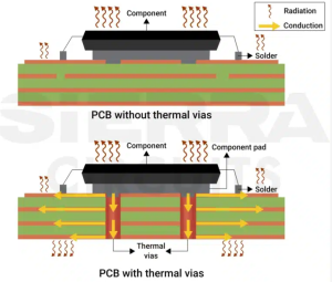
Thermal vias are small, strategically positioned holes filled or plated with conductive material, such as copper, that connect the different layers of a PCB. These pathways allow heat to move away from high-temperature zones—typically where power components reside—and dissipate it across larger surface areas or heat sinks. Although often invisible at first glance, thermal vias play an indispensable role in ensuring the reliability and longevity of electronic assemblies.
In traditional PCB configurations, heat generated by high-performance components can quickly accumulate, especially in dense multilayer boards. Without a proper thermal management strategy, this heat build-up can lead to performance degradation, shortened component lifespan, or even catastrophic failure. Therefore, managing thermal flow is no longer an optional step in PCB design—it has become a necessity. This is where thermal vias shine. They serve as a thermal bridge, connecting the heat-generating layers or surfaces to thermal reliefs or heat dissipation planes located elsewhere on the board.
From a historical perspective, the incorporation of thermal vias began as a response to the limitations of passive cooling techniques like airflow or simple heat sinks. With the rise of high-density interconnects (HDI) and system-on-chip (SoC) technologies, the need to manage heat within the PCB itself became urgent. As power density increased and component footprints shrank, engineers needed new methods to ensure efficient heat evacuation from critical zones. Thermal vias provided a scalable, cost-effective answer that could be integrated into standard fabrication processes.
What makes thermal vias particularly compelling is their passive nature. Unlike active cooling systems that rely on fans, pumps, or thermoelectric modules, thermal vias have no moving parts, consume no energy, and add minimal weight to the final product. They can be implemented with great precision during PCB manufacturing, offering tailored solutions for different heat profiles and component layouts. In multilayer PCBs, thermal vias can be stacked, staggered, or clustered depending on the thermal requirements of specific regions.
Despite their many advantages, thermal vias are not a one-size-fits-all solution. Their effectiveness depends on several variables, such as via diameter, plating thickness, the number of vias, their spacing, and the conductivity of the fill material. Overuse of thermal vias may lead to increased manufacturing complexity and cost, while underuse can compromise thermal performance. Therefore, it is essential to strike the right balance during the design phase.
The manufacturing of thermal vias also involves specialized processes that differ from standard signal or ground vias. These may include via-in-pad technology, conductive paste filling, or resin encapsulation followed by planarization. Each method has its trade-offs in terms of thermal conductivity, mechanical stability, and cost. Careful consideration must also be given to avoid thermal vias introducing unwanted electrical coupling or interfering with signal integrity in high-frequency designs.
From a personal perspective, I believe that thermal vias represent one of the most elegant solutions in modern electronic thermal design. Their simplicity belies their critical function. In my experience, the most successful PCB projects I’ve participated in are those where thermal management is addressed early in the design cycle, and thermal vias are strategically leveraged rather than retrofitted as an afterthought. When used thoughtfully, thermal vias enable the creation of compact, high-power systems without the burden of bulky or noisy active cooling mechanisms.
Another often-overlooked aspect is how thermal vias contribute to product safety and regulatory compliance. In sectors like automotive, aerospace, and medical electronics, devices are subjected to rigorous thermal and environmental testing. A robust via-based heat management system can make the difference between passing or failing these tests. Additionally, thermal vias can improve the Mean Time Between Failures (MTBF), an important metric for mission-critical applications.
Looking ahead, the role of thermal vias in PCB manufacturing is poised to grow even more significant. Emerging technologies such as wide-bandgap semiconductors (like GaN and SiC), which operate at higher power densities, will demand even more effective thermal solutions. Likewise, as flexible and wearable electronics become mainstream, embedding thermal vias in unconventional substrates will present new challenges and opportunities for innovation.
In summary, thermal vias may seem like a minor detail in the grand architecture of PCB manufacturing, but they play a disproportionately large role in ensuring system performance, reliability, and efficiency. Their ability to manage heat passively, without compromising board space or adding mechanical complexity, makes them an essential tool in the modern PCB designer’s arsenal. As we delve deeper into the various technical, material, and application-specific aspects of thermal vias in the sections to follow, we will uncover why these tiny holes are a big deal in the world of electronics.
Thermal Vias
2. Understanding the Thermal Challenges in PCB Design
Thermal management has always been a central consideration in electronics design, but its importance has grown exponentially with the evolution of complex and densely populated printed circuit boards (PCBs). As we push the limits of miniaturization and performance, heat has become not only a byproduct but also a serious design challenge that can directly impact functionality, safety, and product lifespan.
In modern PCBs, especially those used in high-performance or compact environments, multiple components operate simultaneously and continuously, generating considerable heat. Without an effective dissipation path, this heat accumulates and causes temperature rises that can lead to various issues such as signal degradation, mechanical stress, and thermal fatigue. Worse yet, continuous thermal strain can permanently damage sensitive components or the PCB substrate itself.
Several common design factors contribute to thermal buildup:
-
High Component Density: As devices become smaller and more powerful, the physical space available for components decreases. This compression increases the local thermal density and creates hotspots.
-
Increased Power Consumption: High-performance processors, power amplifiers, and RF components draw more current, which in turn generates more heat that must be channeled away.
-
Multilayer Stack-Ups: In many cases, signal layers, power planes, and ground planes are sandwiched between insulating dielectric layers, trapping heat within the board core.
-
Limited Airflow: Enclosures designed for compactness often restrict airflow, reducing the effectiveness of convection-based cooling.
-
Environmental Conditions: Devices used in extreme environments—such as automotive, aerospace, or outdoor applications—are subjected to higher ambient temperatures, which worsen thermal stress.
To mitigate these challenges, engineers must adopt a comprehensive thermal strategy that addresses both the generation and removal of heat. This includes selecting components with better thermal characteristics, positioning heat-generating components away from each other, incorporating thermal relief pads, and—most importantly—employing efficient heat transfer mechanisms like thermal vias.
While passive heat sinks and fans are often used in systems with greater space and budget, they are not always viable in compact designs. That’s where thermal vias become crucial. By creating conductive pathways between the heat source and larger copper areas or external heat spreaders, thermal vias offer a low-resistance path for heat flow. Their integration must be considered from the early stages of layout design, especially in multilayer boards where core temperature management is more complex.
Another challenge in thermal design is predicting heat flow accurately. Unlike electrical design, where resistance and current can be easily calculated, thermal behavior is influenced by a variety of parameters including material conductivity, PCB stack-up, via construction, and component distribution. Thermal vias, though relatively simple in appearance, are influenced by all of these parameters and can significantly alter the thermal profile of the board.
One important consideration is thermal bottlenecking, which occurs when heat is unable to move quickly enough through the internal layers of a PCB. In such cases, adding more copper alone may not solve the issue. Without well-placed thermal vias, the heat will linger, increasing the risk of localized thermal damage. Understanding the heat flow path and identifying thermal choke points early in the design phase can prevent future reliability problems.
It is also worth noting that thermal expansion mismatch between materials—like copper vias, FR-4 substrate, and solder joints—can cause delamination, micro-cracking, and other mechanical failures under cyclic thermal loading. Proper design of thermal vias helps distribute heat more evenly, reducing the likelihood of such failures. This is particularly important for products expected to undergo thermal cycling or long-term continuous operation.
In some designs, the lack of thermal consideration leads to over-engineering later on, such as adding excessive heat sinks or forced cooling systems, increasing cost and complexity. Instead, addressing the issue with well-placed thermal vias can lead to more elegant and efficient solutions. For example, in LED lighting boards, where heat dissipation is a critical performance factor, thermal vias help transfer heat from the LED junction to the metal-core substrate below, enabling longer life and higher brightness.
From a design philosophy standpoint, thermal challenges shouldn’t be treated as an isolated concern but as a multi-dimensional problem that affects electrical, mechanical, and reliability domains. Thermal vias serve as a bridge between all these aspects—physically and metaphorically—by offering an integrated solution that enhances performance without additional active elements.
In my own design experience, I’ve encountered projects where thermal failure analysis revealed that poor thermal via planning was at the heart of repeated system failures. In one such case, a high-frequency power board showed consistent overheating despite the presence of thick copper planes. Upon deeper investigation, it became clear that the heat wasn’t being adequately transferred from the component layer to the internal plane because thermal vias had been sparsely used. A simple redesign with optimized via placement reduced surface temperature by over 15°C under full load conditions.
To conclude this section, understanding the thermal challenges in PCB design is not just about knowing what causes heat; it’s about predicting where it will go and how quickly it can be removed. Thermal vias, when thoughtfully implemented, offer a highly efficient, scalable, and passive method to mitigate these challenges. As we will explore in later sections, the structural properties, placement strategies, and manufacturing techniques of thermal vias can drastically impact their thermal effectiveness—and ultimately, the overall success of the product.
3. Thermal Vias in PCB Manufacturing: Structure and Functionality
To fully appreciate the impact of thermal vias in PCB manufacturing, it’s essential to delve into their structural properties and functional mechanisms. While they may appear to be simple drilled holes filled or plated with conductive material, thermal vias are, in reality, critical architectural features that dictate how effectively heat can be moved across and away from high-power components. Their design must account for electrical isolation, thermal transfer, mechanical reliability, and manufacturability.
3.1 Basic Anatomy of Thermal Vias
At their core, thermal vias are vertical conduits connecting one layer of a PCB to another. They typically consist of a small cylindrical hole, drilled through the PCB substrate, then plated with copper or filled with a conductive material to create a continuous thermal path. Their structure can vary significantly depending on their specific function, the number of layers in the PCB, and the operating environment.
Common attributes of thermal vias include:
-
Via Diameter: Typically ranging from 0.2 mm to 0.5 mm, though smaller microvias are used in HDI boards.
-
Plating Thickness: The copper lining of the via wall must be thick enough to ensure sufficient thermal conductivity without compromising mechanical integrity.
-
Via Fill: Vias can be left empty, filled with metal paste, or plugged with resin, depending on the desired thermal and structural outcomes.
-
Annular Ring: This is the pad area around the via on each layer, which ensures solid connectivity and manufacturing tolerance.
These structural elements affect the heat flow from the component pad to internal copper planes, and eventually to heat spreaders or external radiators.
3.2 The Thermal Function of Thermal Vias
Thermal vias act as highways for heat. When a component like a voltage regulator or processor generates heat, that energy is conducted through the solder pad into the vias and then spreads into broader copper planes—usually inner power or ground layers. Because copper has a high thermal conductivity (~400 W/m·K), the heat is quickly moved away from the source and diffused across the PCB.
In a typical multilayer design, thermal vias connect the surface-mounted device (SMD) pad on the top layer to large copper pours or dedicated heat-spreading layers inside or on the bottom layer. These vias may be deployed in arrays beneath the component, forming a matrix of parallel thermal paths that dramatically reduce thermal resistance.
The effectiveness of this heat transfer is governed by Fourier’s Law, where the heat transfer rate is proportional to the cross-sectional area of the via and inversely proportional to its length (or depth). Therefore, more vias (greater area) and shorter path lengths translate to better thermal conduction.
3.3 Fill Types and Their Implications
The way a thermal via is filled or treated significantly influences its performance. In general, the following via types are employed in thermal design:
-
Plated Through-Hole (PTH) Thermal Vias: These are the most common. The hole is simply plated with copper during fabrication. They offer a balance between performance and cost.
-
Filled Thermal Vias: These are filled with conductive paste or epoxy (and sometimes copper electroplated afterward), offering enhanced thermal and mechanical properties. They are often used in high-reliability applications.
-
Via-in-Pad Thermal Vias: In this configuration, the via is placed directly beneath the SMD pad and either capped or filled to allow for flat soldering. This allows for efficient heat transfer directly from the component to the via network.
-
Blind and Buried Vias: Used in high-density or HDI PCBs, these vias do not extend through the entire board but connect specific layers, enabling tailored thermal management without consuming excessive board space.
3.4 Role in Thermal and Mechanical Stability
Thermal vias also improve mechanical reliability by balancing temperature distribution. Uneven heating on a board can lead to warping, expansion, or contraction at different rates, which is particularly problematic in multilayer boards where different materials expand at different rates. Thermal vias reduce these gradients by spreading heat evenly, minimizing mechanical stress.
Moreover, thermal vias help maintain the temperature differential between various sections of the PCB. In power electronics, for instance, maintaining thermal uniformity ensures that all components function within their optimal operating temperature range. This consistency is crucial to prevent sudden failures due to thermal shocks or hotspot-induced degradation.
3.5 Limitations and Design Considerations
Despite their value, thermal vias must be used thoughtfully. Excessive use can lead to:
-
Increased Cost and Complexity: More vias require more drilling, filling, and inspection during manufacturing.
-
Reduced PCB Real Estate: Densely packed vias can limit space for signal routing, especially on small or constrained boards.
-
Thermal Leakage: In mixed-signal or analog designs, thermal vias may unintentionally connect thermally sensitive analog regions with hotter power zones, disturbing circuit operation.
Thus, careful modeling—often using thermal simulation tools like Ansys or COMSOL—is necessary to strike the right balance.
From my own project experience, I’ve found that early simulation and cross-functional collaboration between mechanical and electrical engineers lead to better thermal via designs. For example, in one telecommunications project, our team reduced operating temperatures by over 20% simply by replacing non-filled vias with metal-filled variants and repositioning them closer to the component’s power pad, without needing to modify the external heat sink design.
4. Material Considerations for Thermal Vias in PCB Manufacturing
Selecting appropriate materials is a cornerstone of effective thermal via implementation in PCB manufacturing. Thermal vias rely on efficient heat conduction through their structure, which involves multiple materials—each contributing to or potentially limiting thermal performance. Understanding the thermal, electrical, and mechanical properties of these materials enables engineers to design vias that perform reliably under varying conditions, from consumer-grade electronics to mission-critical aerospace systems.
4.1 Copper as the Standard for Thermal Vias
Copper remains the undisputed standard for the conductive walls of thermal vias. Its high thermal conductivity—approximately 400 W/m·K—makes it an ideal choice for rapidly transferring heat from hot components into internal copper planes or external sinks.
Beyond its thermal performance, copper also brings additional benefits:
-
Excellent Electrical Conductivity: Often useful when thermal vias double as grounding vias.
-
Mechanical Stability: Copper-plated vias maintain structural integrity even under temperature fluctuations.
-
Process Compatibility: Copper is fully compatible with standard electroplating and PTH (plated through-hole) fabrication processes.
However, copper’s cost and weight must be considered, especially in applications that require very high via density or low-weight materials (e.g., in aerospace designs).
4.2 Thermal Interface Materials (TIMs) in Via Fill Applications
While many thermal vias are left as plated-through holes, performance can often be improved by filling them with thermal interface materials (TIMs). These materials enhance thermal conduction and improve structural reinforcement, particularly in via-in-pad designs or boards expected to undergo thermal cycling.
Common fill materials include:
-
Conductive Epoxies: These are often loaded with silver or other conductive particles to enhance thermal transfer. They are typically used in high-reliability and military-grade PCBs.
-
Sintered Metal Pastes: Advanced metal pastes, including silver or copper-based sintered materials, offer excellent thermal conductivity and long-term reliability under high-temperature conditions.
-
Resin Fills with Copper Cap Plating: In cost-sensitive applications, epoxy resins are used to fill the via and then capped with a copper layer. This creates a planar surface for soldering and still provides some thermal benefit.
TIM selection must consider thermal conductivity, CTE (coefficient of thermal expansion) compatibility with surrounding materials, curing behavior, and long-term stability.
4.3 Substrate Materials and Their Impact on Thermal Vias
Thermal vias are only one part of the heat dissipation chain. Their effectiveness is also influenced by the surrounding substrate materials, which vary significantly in thermal conductivity.
-
FR-4 (Glass-reinforced Epoxy Resin): This is the most common PCB substrate material. However, it has relatively poor thermal conductivity (~0.3–0.4 W/m·K). In designs using FR-4, thermal vias become especially critical to bypass the insulating nature of the substrate.
-
High-Tg Epoxies and Polyimides: These materials perform better under thermal stress but still do not match the thermal conductivity of metal-core or ceramic options.
-
Metal-Core PCBs (MCPCBs): Often used in LED and power applications, these have aluminum or copper backing. Thermal vias in these designs connect top-layer heat sources directly to the metal core, drastically improving thermal dissipation.
-
Ceramic Substrates: In high-frequency and RF applications, substrates like aluminum nitride or beryllium oxide offer excellent thermal properties. Here, thermal vias can be reduced or supplemented, depending on layout requirements.
Matching the thermal via structure with the substrate’s properties ensures that heat is not simply “bottlenecked” at the via exit point.
4.4 Plating Thickness and Conductivity
The plating thickness of a thermal via’s inner wall has a direct impact on its thermal performance. Thicker plating increases the surface area for conduction and reduces thermal resistance. However, excessive plating can lead to:
-
Reduced inner diameter, affecting fill quality or solder wicking
-
Mechanical stress buildup during thermal cycling
-
Increased fabrication time and cost
A typical balance is 25–35 microns of copper plating on the via wall, which ensures sufficient conductivity without adding unnecessary complexity.
In some cases, double-pass plating or enhanced via fill processes are used to achieve superior thermal conductivity, especially when high-current paths coincide with thermal pathways.
4.5 Coefficient of Thermal Expansion (CTE) Compatibility
CTE mismatch is a hidden but critical factor in thermal via material selection. When copper (CTE ~17 ppm/°C) is used within FR-4 or polyimide substrates (CTE ~70 ppm/°C or more), repeated thermal cycling can cause delamination, cracking, or via barrel fatigue. This is especially problematic in harsh environments such as automotive under-hood electronics or industrial automation systems.
To mitigate this:
-
Fill materials should be selected for close CTE matching.
-
Use of compliant layers or stress-relief patterns around high-via-density areas can absorb differential expansion.
-
In extreme cases, switch to ceramic-filled or low-CTE laminate systems to maintain structural stability.
4.6 Environmental and Manufacturing Considerations
Some materials, especially advanced metal pastes and high-thermal-conductivity fillers, may require specialized manufacturing processes. For example:
-
High-temperature sintering for silver paste
-
Controlled curing cycles for conductive epoxies
-
Cleanroom processing for ceramic substrates
Additionally, RoHS compliance, halogen-free regulations, and long-term aging resistance must be considered when selecting thermal via materials, especially in consumer and medical devices.
In my own design projects, the choice of materials has often been the determining factor in thermal management success. On one occasion, substituting a low-cost thermal epoxy for a higher-grade metal-filled variant in thermal vias resulted in a 12% drop in operating temperature and significantly improved product lifetime estimates in accelerated aging tests.
5. Design Optimization Strategies for Thermal Vias in PCB Manufacturing
In modern PCB layouts, thermal vias must be thoughtfully integrated into the overall design strategy to ensure not just functional heat dissipation but also manufacturing efficiency and electrical performance. Design optimization encompasses geometric parameters, via placement, pad integration, layer connectivity, and the use of thermal simulations to refine and validate concepts before production. The goal is to maximize heat transfer while balancing space, cost, and signal integrity constraints.
5.1 Geometric Optimization of Thermal Vias in PCB Manufacturing
The geometry of each thermal via significantly influences its thermal conductivity. Key geometric parameters include:
-
Via Diameter: Larger vias can carry more heat, but take up more PCB real estate. Typical diameters range from 0.2 mm to 0.5 mm for standard thermal vias.
-
Aspect Ratio: This is the ratio of PCB thickness to via diameter. Lower aspect ratios favor better plating uniformity and structural reliability. An aspect ratio below 8:1 is typically preferred.
-
Via Wall Thickness: The copper plating thickness along the via barrel affects the thermal path. Optimizing wall thickness (usually between 25–35 microns) ensures a good tradeoff between thermal performance and fabrication feasibility.
Designers should avoid creating thermal vias with dimensions that strain fabrication tolerances, as this can lead to higher defect rates and poor plating coverage.
5.2 Optimal Placement Patterns for Thermal Vias in PCB Manufacturing
Placement of thermal vias matters just as much as their material and geometry. Thermal dissipation is most effective when the vias are:
-
Directly beneath heat-generating components, such as power ICs, MOSFETs, or voltage regulators.
-
Evenly distributed across the copper pad under the component to avoid heat accumulation at any one point.
-
Connected to large internal or bottom copper planes, which act as thermal reservoirs or heat sinks.
Designers frequently use arrays of thermal vias in grid or honeycomb patterns. A typical density is 4–9 vias per square centimeter under high-power devices. However, diminishing returns set in beyond a certain density, and thermal performance gains plateau.
5.3 Integration of Thermal Vias in Pad Designs
For surface-mount packages such as QFNs or power BGAs, vias are often placed directly in thermal pads (commonly known as via-in-pad). While this method provides direct thermal conduction, it introduces challenges:
-
Solder Wicking: During reflow, solder may be drawn down into the via, leading to poor solder joints or voids.
-
Planar Irregularities: If vias are not properly filled and capped, they can result in uneven mounting surfaces.
To address these issues, via filling and planarization techniques such as copper or epoxy fill followed by copper capping are employed. This ensures both effective heat transfer and reliable soldering.
5.4 Multi-Layer Heat Spreading via Thermal Vias in PCB Manufacturing
Connecting thermal vias to multiple internal copper layers amplifies their cooling capacity. This strategy transforms the PCB into a vertical heat spreader by:
-
Allowing heat to distribute across several copper planes.
-
Enabling multiple exit pathways to thermal dissipation features, such as metal backplates or external heat sinks.
Designers should ensure electrical isolation if thermal vias intersect with power or signal planes. Use of isolated thermal islands or stitching techniques around ground areas helps mitigate unwanted coupling or noise propagation.
5.5 Using Thermal Simulations for Optimizing Thermal Vias in PCB Manufacturing
Before finalizing PCB designs, thermal simulations are an indispensable tool. Simulation software such as ANSYS, SolidWorks Thermal, and Mentor Graphics FloTHERM allow designers to:
-
Model heat flow across the board and identify hotspots.
-
Evaluate various via densities and patterns without fabricating multiple prototypes.
-
Simulate real-world conditions, including airflow, power cycling, and environmental temperatures.
By analyzing heat maps and thermal gradients, designers can iteratively refine thermal via configurations. In one project I contributed to, simulation revealed that reducing via diameter by 10% and increasing density improved the temperature gradient under a power amplifier by over 8°C—an improvement that would’ve gone unnoticed without modeling.
5.6 Design Trade-offs Involving Thermal Vias in PCB Manufacturing
Despite their benefits, thermal vias also introduce design trade-offs that must be balanced carefully:
-
Signal Integrity: High-density via arrays may interfere with high-speed signals if not isolated properly.
-
Board Space: Dense via arrays occupy valuable space, especially in compact layouts.
-
Manufacturing Cost: Filled, capped, and blind/buried thermal vias significantly raise fabrication costs.
-
Reliability vs. Performance: Sometimes, adding more vias improves heat removal but creates mechanical stress or manufacturing complexity.
A well-optimized design balances all these factors to create a solution that is thermally effective without compromising functionality or yield.
6. Manufacturing Challenges of Thermal Vias in PCB Manufacturing
While thermal vias offer significant thermal performance advantages in PCB designs, their incorporation into manufacturing processes introduces a distinct set of challenges. From drill accuracy to via filling, every step requires careful control to ensure the functionality and reliability of the finished board. In high-volume production or complex multilayer PCBs, these issues are further magnified. This section explores the key manufacturing hurdles and the strategies used to mitigate them.
6.1 Drilling Precision and Alignment Issues for Thermal Vias in PCB Manufacturing
One of the foundational steps in creating thermal vias is mechanical or laser drilling. The quality and accuracy of this step determine the integrity of the via throughout its life cycle. Common challenges include:
-
Misalignment between via drills and internal copper layers, which can degrade heat transfer.
-
Drill wander in multilayer stacks, especially in thick or high-aspect-ratio boards.
-
Burr formation, which can interfere with plating and lead to voids or poor adhesion.
To counter these, manufacturers use high-precision CNC drilling systems with real-time position correction, X-ray registration systems, and laser direct imaging (LDI) for fine-pitch via arrays. For smaller vias (<0.2 mm), UV or CO₂ lasers offer better precision.
6.2 Challenges in Plating Thermal Vias in PCB Manufacturing
Copper plating is central to the effectiveness of thermal vias. However, consistent and defect-free plating across all vias—especially those with high aspect ratios—is technically demanding.
Issues may include:
-
Void formation: Air pockets or chemical residue trapped in the via can prevent copper from forming a continuous path.
-
Thin plating at the via center due to insufficient solution flow during electroplating.
-
Overplating, which narrows the via opening or leads to cracking due to internal stress.
To address these, advanced PCB shops use pulse electroplating or periodic reverse plating techniques, along with agitated plating tanks to enhance solution penetration. In addition, pre-treatment processes such as desmear and deionized water rinsing help ensure optimal surface preparation.
6.3 Via Filling and Capping Complications in Thermal Vias in PCB Manufacturing
When thermal vias are used in via-in-pad designs or require structural reinforcement, they must be filled and capped. Each of these steps can present difficulties:
-
Void formation during filling: Uneven fill can trap air, reduce thermal conductivity, or cause warping during reflow.
-
Capping irregularities: Poor flatness on capped vias leads to coplanarity issues during component mounting.
-
Resin shrinkage: Certain epoxy fills may contract during curing, inducing mechanical stress or delamination.
High-end fabrication facilities utilize vacuum-assisted filling, low-shrinkage resin systems, and precision planarization equipment to maintain surface uniformity. Some manufacturers also use metallic fill materials to boost thermal conductivity, though this introduces additional cost and complexity.
6.4 Thermal Stress and Reliability Testing for Thermal Vias in PCB Manufacturing
Once manufactured, PCBs with thermal vias must undergo reliability testing to ensure they perform under thermal cycling and mechanical load. Challenges in this phase include:
-
Barrel cracking: Differential expansion between copper and substrate materials can cause microcracks in the via walls.
-
Pad lifting or delamination: Caused by poor adhesion or excessive thermal expansion forces.
-
CTE mismatch failures, especially in multilayer designs or hybrid material stacks.
Accelerated aging tests such as thermal shock, temperature cycling, and power cycling are used to qualify thermal via reliability. Cross-sectioning and X-ray inspection are also employed to verify internal via integrity.
In my own experience managing prototyping for automotive ECUs, we encountered barrel cracks in thermal vias during thermal cycling above 150°C. The issue was traced back to insufficient wall plating and aggressive via fill materials. Refining the plating process and switching to a CTE-compatible epoxy mitigated the failure in subsequent runs.
6.5 Yield Loss and Cost Escalation in Thermal Vias in PCB Manufacturing
Incorporating thermal vias—especially in high-density or high-performance PCBs—can increase manufacturing costs and lower yield due to:
-
Additional fabrication steps (drilling, plating, filling, capping)
-
Increased inspection complexity
-
Tighter process tolerances, which reduce error margins
To maintain a viable cost-performance ratio, design engineers often collaborate closely with PCB manufacturers to:
-
Use via arrays only where needed, reducing unnecessary complexity.
-
Opt for standard via types (non-filled, non-capped) where possible.
-
Simplify layer stack-ups, reducing interconnect layers and via transitions.
6.6 Environmental and Regulatory Considerations in Thermal Vias in PCB Manufacturing
Modern electronics manufacturing must comply with regulations such as:
-
RoHS (Restriction of Hazardous Substances)
-
REACH (Registration, Evaluation, Authorisation and Restriction of Chemicals)
-
WEEE (Waste Electrical and Electronic Equipment)
Thermal via fabrication processes—especially those involving metal pastes, epoxy fills, and cleaning solvents—must align with these standards. Manufacturers are increasingly moving toward halogen-free, low-VOC, and lead-free alternatives, though these materials may behave differently in plating and thermal conduction.
In particular, lead-free soldering imposes higher reflow temperatures (up to 260°C), requiring thermal vias to withstand additional thermal stress. Material selection, plating thickness, and CTE compatibility all become more critical under such conditions.
7. Testing and Validation of Thermal Vias in PCB Manufacturing
The performance of thermal vias cannot be fully guaranteed by design and fabrication alone—they must undergo rigorous testing and validation processes to confirm that they meet thermal, mechanical, and electrical reliability expectations. In this section, we explore industry-standard testing methodologies, simulation practices, real-world thermal profiling, and failure analysis used to validate thermal via performance in PCB manufacturing.
7.1 Importance of Functional Testing for Thermal Vias in PCB Manufacturing
Thermal vias play a critical role in heat management, and if improperly implemented, they can lead to elevated component temperatures, degraded performance, and reduced system reliability. Functional testing focuses on assessing whether thermal vias are performing their intended heat dissipation role in a live or simulated operating environment.
Key functional tests include:
-
Thermal resistance measurement between the component pad and the opposite side of the PCB or internal copper planes.
-
Heat rise tracking under specific current loads.
-
Component temperature monitoring using embedded sensors or thermocouples.
Such tests help determine whether thermal vias are effectively conducting heat as modeled. For high-power applications like LED boards, DC-DC converters, or RF modules, this testing is not optional—it is mission-critical.
7.2 Thermographic Imaging for Thermal Vias in PCB Manufacturing
One of the most effective validation tools is infrared thermography, which captures real-time heat maps of a functioning PCB. These images visualize temperature distribution and allow engineers to:
-
Identify hotspots or underperforming thermal via areas.
-
Compare pre- and post-design changes in via arrays.
-
Validate simulation models with physical results.
Thermographic testing is usually conducted in an environmental chamber that mimics field conditions (e.g., airflow, ambient temperature, and load). By combining imaging with thermocouples, engineers can validate heat spreading effectiveness and confirm whether the vias are acting as intended thermal conduits.
7.3 Cross-Sectional Analysis of Thermal Vias in PCB Manufacturing
To evaluate the physical integrity of thermal vias post-manufacture, cross-sectional microsectioning is used. This involves cutting a precise slice through a sample via and inspecting it under a microscope for:
-
Plating uniformity and thickness
-
Presence of voids or cracks
-
Via fill consistency (especially for filled and capped designs)
Such analysis helps manufacturers assess quality control, verify compliance with IPC standards (such as IPC-6012 or IPC-TM-650), and identify root causes of any failures observed during reliability tests.
In a recent project, microsectioning of thermally critical vias revealed underplating at the center barrel, which was not apparent during electrical continuity testing but led to thermal failure under prolonged load. The plating process was then recalibrated to improve current density uniformity.
7.4 Accelerated Life Testing of Thermal Vias in PCB Manufacturing
To ensure thermal vias withstand operational stress over time, accelerated life testing (ALT) is conducted. This includes:
-
Thermal cycling tests, where the board is exposed to repeated heating and cooling cycles between -40°C to +125°C or higher.
-
Power cycling, which stresses vias by continuously toggling high current loads.
-
High Temperature Operating Life (HTOL) testing, especially for automotive and aerospace PCBs.
Such tests simulate long-term fatigue and help predict Mean Time to Failure (MTTF). Failures in thermal vias often manifest as gradual temperature rises due to microcracks, which increase thermal resistance.
7.5 In-Circuit Testing and Boundary Scan for Thermal Vias in PCB Manufacturing
Although in-circuit testing (ICT) is mainly used to validate electrical functionality, it can also provide insights into thermal via integrity by:
-
Detecting resistive anomalies in via-connected nets.
-
Measuring voltage drops that may correlate with poor via conductivity.
-
Triggering targeted thermal inspections where electrical anomalies are found.
In designs where thermal vias double as grounding or power connections, ICT becomes an essential verification tool. Boundary scan (JTAG) can also be used in highly integrated designs to perform connectivity checks across multi-layer via structures.
7.6 Correlating Simulation with Empirical Data for Thermal Vias in PCB Manufacturing
Simulation plays a central role in modern PCB development, but simulations must be grounded in reality. Validation involves comparing predicted thermal behavior with actual test data to:
-
Refine material properties and boundary conditions in simulation models.
-
Adjust via dimensions and densities to better match measured performance.
-
Validate software tools like ANSYS Icepak, COMSOL Multiphysics, or Mentor Graphics FloTHERM.
Simulation-empirical correlation helps ensure that future designs benefit from more accurate virtual prototyping, reducing the number of costly physical iterations needed.
7.7 Common Failure Modes Detected During Testing of Thermal Vias in PCB Manufacturing
Testing thermal vias often reveals various failure modes, including:
-
Partial or full delamination around via walls due to poor adhesion or thermal stress.
-
Microvoids inside via fills that compromise heat transfer.
-
Via barrel cracking due to mechanical expansion mismatch.
-
Uneven copper plating that leads to electrical and thermal inconsistencies.
Understanding and cataloging these failure patterns is essential for establishing robust design guidelines and manufacturing process controls.
8. Comparative Analysis of Thermal Vias with Alternative Thermal Management Techniques in PCB Manufacturing
In modern electronic assemblies, managing heat is a fundamental design challenge. While thermal vias are widely used and highly effective, they are not the only thermal management strategy available. This section provides a critical comparative analysis between thermal vias and other prevalent thermal dissipation solutions, assessing their performance, complexity, cost, and practical integration in PCB manufacturing. The goal is to highlight where thermal vias excel, where they fall short, and when alternative techniques may be preferable.
8.1 Comparing Thermal Vias with Heat Sinks in PCB Manufacturing
Heat sinks are external structures attached to heat-generating components or directly to the PCB to dissipate thermal energy via conduction and convection. Compared to thermal vias:
| Aspect | Thermal Vias | Heat Sinks |
|---|---|---|
| Location | Embedded in PCB layers | External, mounted on top |
| Heat Dissipation Path | Through PCB to inner/outer copper planes | From component surface to ambient |
| Complexity | Requires multilayer stackup, via drilling | Requires mechanical attachment |
| Cost | Moderate | Moderate to high (especially for custom sinks) |
| Effectiveness | Excellent for localized, layered heat | Excellent for surface dissipation |
In high-power applications, thermal vias and heat sinks are often combined, with the vias conducting heat away from components and the sink dispersing it into the surrounding air.
8.2 Comparing Thermal Vias with Thermal Pads in PCB Manufacturing
Thermal interface pads (such as thermal grease, gap fillers, or phase change materials) are used to bridge the gap between a component and a heat sink or metal baseplate.
| Aspect | Thermal Vias | Thermal Pads |
|---|---|---|
| Integration | Internal to PCB | External material placed between surfaces |
| Thermal Conductivity | High (through copper) | Variable (1–10 W/m·K typical) |
| Application Focus | Permanent, structural design feature | Flexible, field-adjustable |
| Durability | Excellent (fixed) | Degrades over time (thermal cycling) |
While thermal pads offer design flexibility and ease of assembly, they are not structurally integrated and are prone to long-term degradation. In contrast, thermal vias are permanent and stable over the product’s lifecycle.
8.3 Comparing Thermal Vias with Embedded Copper Coins in PCB Manufacturing
Embedded copper coins are thick copper slugs inserted into the PCB under high-power components to provide an ultra-low thermal resistance path.
| Aspect | Thermal Vias | Copper Coins |
|---|---|---|
| Manufacturing Complexity | Moderate | High (special routing, insertion) |
| Heat Transfer Capacity | Good | Very High (bulk copper mass) |
| Footprint Impact | Minimal | Large |
| Cost | Moderate | High |
Copper coins outperform thermal vias in extreme thermal scenarios, such as high-current power electronics. However, their complexity, size, and cost make them less appealing for standard consumer electronics.
8.4 Comparing Thermal Vias with Metal Core PCBs in PCB Manufacturing
Metal Core PCBs (MCPCBs) use a metal base layer (usually aluminum) instead of a fiberglass substrate to conduct heat more effectively.
| Aspect | Thermal Vias | Metal Core PCBs |
|---|---|---|
| Core Material | FR4 + copper vias | Metal (aluminum, copper) base |
| Thermal Conductivity | Via-dependent | Uniformly high |
| Design Flexibility | High (multilayer, complex stackups) | Limited (single or few layers) |
| Weight & Thickness | Lower | Higher |
MCPCBs are optimal for LED lighting and power converters, but thermal vias remain more versatile in multilayer digital and RF boards, especially when signal integrity and compactness are critical.
8.5 Comparing Thermal Vias with Graphene and Advanced Materials in PCB Manufacturing
With advances in nanomaterials, graphene-based heat spreaders and diamond composites are being explored for next-gen thermal management.
| Aspect | Thermal Vias | Advanced Materials |
|---|---|---|
| Maturity | Fully industrialized | Emerging, experimental |
| Thermal Conductivity | ~400 W/m·K (copper) | 1000–5000 W/m·K (graphene, diamond) |
| Cost and Availability | Economical | Expensive and limited |
| Manufacturing Risk | Low | High (compatibility, bonding, aging) |
Although promising, graphene and related technologies are not yet practical replacements for thermal vias in mass PCB manufacturing. They remain under research for niche, high-performance applications such as space-grade electronics.
8.6 When Thermal Vias Outperform Other Solutions in PCB Manufacturing
Thermal vias shine in scenarios such as:
-
Compact multilayer PCBs with vertical heat dissipation needs.
-
Designs with tight mechanical constraints where heat sinks or thick cores aren’t feasible.
-
High-reliability applications requiring robust, long-term thermal stability.
-
Cost-sensitive projects where copper plating and drilling are cheaper than exotic materials.
When designed optimally and in conjunction with planes or thermal pads, thermal vias offer a balance of performance, manufacturability, and cost-efficiency unmatched by most alternatives.
8.7 Synergistic Use of Thermal Vias and Other Techniques in PCB Manufacturing
In many real-world designs, thermal vias are not used in isolation. Instead, they are part of a broader heat management strategy. Examples include:
-
Vias combined with heat sinks and thermal interface materials in high-power LED modules.
-
MCPCBs with thermal vias beneath power ICs to reduce local temperature spikes.
-
Copper coin embedded designs with via arrays for even heat spreading.
Such hybrid approaches leverage the strengths of each technique, ensuring optimal performance across a wide range of thermal challenges.
9. Design Software and Simulation Tools for Thermal Vias in PCB Manufacturing
In the increasingly complex field of PCB manufacturing, accurately designing and validating thermal vias requires the use of advanced software and simulation tools. These tools help engineers predict thermal performance, optimize via placement, and ensure reliability before committing to costly physical prototypes. This section explores key design software and simulation techniques specifically relevant to thermal vias in PCB manufacturing, highlighting their capabilities, advantages, and practical considerations.
9.1 The Role of CAD Software in Thermal Vias Design for PCB Manufacturing
Computer-Aided Design (CAD) software forms the foundation for PCB layout and via placement. Leading PCB CAD tools such as Altium Designer, Cadence Allegro, and Mentor Graphics PADS provide robust functionality for defining via structures, layer stackups, and copper pours.
-
Thermal via definition: These platforms allow designers to specify via diameter, plating thickness, and drill parameters that directly impact thermal conductivity.
-
Layer stack management: CAD tools enable clear visualization and management of multilayer boards, essential for understanding heat paths involving thermal vias.
-
Integration with electrical design: Thermal vias must be coordinated with signal integrity and power delivery, which CAD tools facilitate by integrating electrical and thermal design considerations.
While CAD software focuses on layout and physical design, it often links to simulation tools for thermal analysis.
9.2 Thermal Simulation Tools for Optimizing Thermal Vias in PCB Manufacturing
Thermal simulation is critical to validate thermal via effectiveness before manufacturing. Popular thermal simulation tools include ANSYS Icepak, COMSOL Multiphysics, and Flotherm.
-
Heat transfer modeling: These tools simulate conduction, convection, and radiation within the PCB stackup, incorporating thermal vias as discrete or distributed thermal conductors.
-
Parametric studies: Engineers can adjust via size, quantity, and distribution to observe effects on hotspot temperatures and thermal gradients.
-
Material property integration: Simulations incorporate the thermal conductivity of copper, substrate materials, and solder mask layers to ensure realistic predictions.
-
Transient and steady-state analysis: Designers assess how quickly heat dissipates during power cycling or under continuous operation.
Simulation output guides decision-making on via density, arrangement, and compatibility with other cooling techniques.
9.3 Integration of Electrical-Thermal Co-Simulation in Thermal Vias Design for PCB Manufacturing
Modern designs increasingly require simultaneous electrical and thermal analysis. Co-simulation tools combine signal integrity and thermal performance modeling to optimize thermal vias without compromising circuit functionality.
-
Electrical performance impact: Thermal vias, especially when numerous, can affect impedance and crosstalk. Co-simulation ensures thermal improvements do not degrade electrical signals.
-
Thermal stress prediction: Co-simulation also predicts thermomechanical stresses induced by temperature gradients near thermal vias, helping to prevent reliability issues.
-
Design trade-offs: Engineers evaluate trade-offs between thermal management and high-speed signal requirements, achieving balanced, manufacturable designs.
Tools such as Cadence Sigrity and Ansys RedHawk enable this integrated approach, vital for complex high-speed PCBs.
9.4 Automated Design and Optimization Algorithms for Thermal Vias in PCB Manufacturing
Recent advances in artificial intelligence and algorithmic optimization have led to automated tools that suggest optimal thermal via configurations.
-
Optimization goals: These tools minimize temperature rise, reduce thermal gradients, and maintain electrical constraints automatically.
-
Machine learning applications: Some platforms use historical data to predict the most effective via placement patterns.
-
Design rule checks: Automated checks ensure thermal vias conform to manufacturability standards, such as drill sizes and plating thicknesses.
Automation accelerates the design cycle and improves thermal via efficiency, especially in large multilayer designs.
9.5 Challenges and Limitations of Design Software and Simulation Tools for Thermal Vias in PCB Manufacturing
Despite their power, design and simulation tools have limitations:
-
Model accuracy: Simplifications in thermal modeling may overlook micro-scale phenomena, such as interface thermal resistance.
-
Computational resource demands: Detailed 3D simulations of complex PCBs can be time-consuming and require high-performance computing resources.
-
User expertise: Effective use requires skilled engineers familiar with both thermal physics and PCB manufacturing constraints.
-
Material data: Accurate thermal properties for novel materials or composites may be unavailable or proprietary, affecting simulation reliability.
Understanding these limitations helps engineers interpret results critically and combine simulation with empirical testing.
9.6 Best Practices for Utilizing Design Software and Simulation Tools in Thermal Vias Optimization
To maximize benefits, engineers should follow best practices:
-
Early simulation: Incorporate thermal simulations early in the design phase to guide via placement and stackup decisions.
-
Iterative refinement: Use simulation feedback to iteratively optimize via parameters, balancing thermal and electrical requirements.
-
Cross-disciplinary collaboration: Thermal engineers, PCB designers, and manufacturing experts should collaborate closely to align simulations with practical constraints.
-
Validation with physical testing: Whenever possible, validate simulations with thermal imaging and temperature measurements on prototypes.
Such integrated workflows reduce risk and enhance the reliability of thermal via implementations.
9.7 Future Trends in Software and Simulation for Thermal Vias in PCB Manufacturing
Looking forward, several trends will shape how software supports thermal via design:
-
Increased use of AI: Enhanced AI-driven optimization will further automate via design, adapting in real-time to design changes.
-
Cloud-based simulation: Cloud platforms will make powerful simulations accessible to smaller companies without large computing infrastructure.
-
Multiphysics integration: Deeper integration of mechanical, electrical, and thermal simulations will improve prediction accuracy.
-
Virtual prototyping: Advanced digital twins will allow real-time thermal management predictions during product operation.
These advances promise to make thermal via design more precise, efficient, and adaptive to future electronic demands.
10. Manufacturing Challenges and Quality Control of Thermal Vias in PCB Manufacturing
Thermal vias are critical for effective heat dissipation in PCBs, but their integration into the manufacturing process poses unique challenges. Ensuring the quality and reliability of thermal vias requires rigorous process control, specialized inspection methods, and continuous improvement efforts. This section examines the key manufacturing challenges associated with thermal vias and discusses quality control techniques essential to delivering robust PCB products.
10.1 Drilling Accuracy and Hole Quality for Thermal Vias in PCB Manufacturing
Drilling the vias accurately is a fundamental step impacting thermal via performance. Challenges include:
-
Precision hole size: Thermal vias often require small diameter holes (e.g., 0.2mm or less) to maximize via density without compromising structural integrity. Achieving consistent drill diameters demands high-quality drill bits and stable drilling equipment.
-
Hole wall smoothness: Rough or damaged hole walls reduce plating adhesion and increase thermal resistance. Optimized drill speeds and proper drill bit maintenance are crucial.
-
Registration alignment: Precise alignment of drilled holes with copper pads is critical to ensure proper electrical and thermal connection.
Failures in drilling can lead to open vias or inconsistent thermal performance.
10.2 Copper Plating Consistency and Its Impact on Thermal Vias in PCB Manufacturing
The copper plating process inside via holes is essential for creating reliable thermal pathways.
-
Uniform plating thickness: Insufficient or uneven plating reduces thermal conductivity and may cause via failure during thermal cycling.
-
Plating adhesion: Good adhesion to the hole walls and copper pads prevents delamination or cracking under thermal stress.
-
Process control: Parameters such as plating bath chemistry, temperature, current density, and time must be tightly controlled.
Regular monitoring of plating thickness using cross-sectional analysis or non-destructive testing helps maintain quality.
10.3 Thermal Via Filling and Via-in-Pad Techniques in PCB Manufacturing
To further enhance thermal performance and surface planarity, thermal vias may be filled or capped.
-
Via filling materials: Conductive epoxy or copper paste can fill vias to improve heat conduction and prevent solder wicking.
-
Via-in-pad technology: Placing thermal vias directly in component pads improves heat transfer but introduces challenges such as solderability and warpage.
-
Manufacturing complexity: Filling and via-in-pad require additional processing steps and inspection, increasing cost and complexity.
Proper process optimization is necessary to balance thermal benefits with manufacturing feasibility.
10.4 Inspection and Testing Methods for Thermal Vias Quality in PCB Manufacturing
Ensuring thermal via quality requires comprehensive inspection and testing protocols.
-
Visual inspection: Automated optical inspection (AOI) can detect surface defects and via placement issues.
-
X-ray inspection: Non-destructive X-ray imaging reveals plating integrity and filling quality inside vias.
-
Cross-section analysis: Destructive cross-sectioning verifies plating thickness and via structure.
-
Thermal performance testing: Thermal imaging and transient thermal measurements validate heat dissipation effectiveness.
Integrating multiple inspection methods helps identify defects early and maintain production standards.
10.5 Common Defects in Thermal Vias and Their Causes in PCB Manufacturing
Understanding typical defects aids in proactive quality management:
-
Voids or air gaps: Caused by incomplete plating or filling, leading to poor thermal conductivity.
-
Delamination: Separation between plating and substrate due to thermal stress or contamination.
-
Cracking: Mechanical stress or thermal cycling can crack plating, breaking thermal paths.
-
Misregistration: Misalignment of vias reduces contact area and heat transfer efficiency.
Root cause analysis and corrective actions are critical to mitigate these defects.
10.6 Process Optimization Strategies for Thermal Vias Manufacturing in PCB Manufacturing
Continuous process improvements enhance thermal via reliability:
-
Drilling parameter optimization: Using appropriate drill bits and feed rates to improve hole quality.
-
Enhanced plating processes: Implementing pulse plating or additive chemistries for better copper deposition.
-
Filling material selection: Choosing materials with high thermal conductivity and compatible expansion coefficients.
-
Operator training: Ensuring skilled personnel to manage sensitive processes and inspections.
Such strategies reduce defects, improve yield, and support high-performance thermal via production.
10.7 Regulatory and Industry Standards Related to Thermal Vias in PCB Manufacturing
Compliance with industry standards ensures consistent quality:
-
IPC standards: IPC-6012 and IPC-6013 specify requirements for via plating and PCB thermal management.
-
RoHS and environmental regulations: Influence materials used in plating and filling processes.
-
Customer-specific standards: High-reliability applications may impose tighter specifications on thermal via quality.
Adherence to these standards facilitates customer trust and product acceptance.
10.8 The Role of Supplier Collaboration in Thermal Vias Quality Assurance in PCB Manufacturing
Manufacturers often rely on external suppliers for drilling, plating, and materials.
-
Supplier qualification: Evaluating and auditing suppliers ensures they meet quality and process requirements.
-
Material traceability: Tracking materials used in plating and filling helps maintain consistency.
-
Collaborative problem-solving: Close communication allows rapid response to defects and continuous improvements.
Strong supplier partnerships are key to achieving superior thermal via manufacturing outcomes.
10.9 Future Developments in Thermal Via Manufacturing and Quality Control
Advances in manufacturing technology will improve thermal via quality:
-
Laser drilling: Offers higher precision and smoother hole walls.
-
Advanced plating techniques: New chemistries and processes can enhance plating uniformity and adhesion.
-
Inline inspection: Real-time monitoring technologies for drilling and plating defects.
-
Smart manufacturing: Integration of AI and IoT for predictive quality control.
These innovations promise to enhance production efficiency and reliability of thermal vias.
This section emphasizes that despite the fundamental role of thermal vias in managing heat, their manufacturing introduces complex challenges that must be carefully managed through precise process control, thorough inspection, and collaboration. Quality control remains paramount to ensure that thermal vias fulfill their critical function in PCB thermal management.
11. Cost Considerations and Design Trade-offs Involving Thermal Vias in PCB Manufacturing
Thermal vias offer crucial thermal management benefits, but incorporating them into PCB designs and manufacturing processes impacts overall cost and complexity. Understanding these cost considerations and balancing design trade-offs is essential to optimize both performance and budget. This section explores the economic aspects of thermal vias and how designers and manufacturers can make informed decisions.
11.1 Material and Process Costs Associated with Thermal Vias in PCB Manufacturing
Adding thermal vias increases the consumption of materials and processing time:
-
Drilling costs: High-density thermal vias require more drilling operations, which increases tool wear, machine time, and maintenance costs.
-
Plating and filling materials: Additional copper plating and via filling materials add to raw material expenses.
-
Inspection and testing: More rigorous quality control for thermal vias adds indirect labor and equipment costs.
While the unit cost increase per PCB might be small, at scale, these costs can become significant.
11.2 Impact of Thermal Via Density and Size on PCB Manufacturing Cost
Thermal via density and via size influence cost in multiple ways:
-
Higher via density: Improves heat dissipation but demands more drilling and plating steps, driving up cost.
-
Smaller via diameters: Require specialized drills and tighter process controls, increasing complexity and yield risks.
-
Trade-off analysis: Designers must balance thermal performance gains against the incremental manufacturing costs.
Careful evaluation of via parameters can help identify the most cost-effective thermal via solution.
11.3 Design Trade-offs Between Thermal Management and Manufacturing Complexity
Incorporating thermal vias involves navigating between thermal needs and manufacturability:
-
Thermal vias vs. board thickness: Adding thermal vias may allow thinner boards but can increase processing difficulty.
-
Via-in-pad vs. traditional vias: Via-in-pad improves thermal conduction but complicates soldering and increases costs.
-
Stack-up considerations: Thermal via placement must not interfere with signal integrity or mechanical strength.
An optimal design considers these trade-offs to meet both performance and cost targets.
11.4 Cost-Benefit Analysis of Thermal Vias in High-Performance Applications
For high-reliability or high-power PCBs, the benefits of thermal vias often justify the added cost:
-
Enhanced device lifespan: Improved thermal management reduces failure rates and warranty claims.
-
Performance optimization: Maintaining temperature limits allows devices to operate at higher speeds or power.
-
Reduced cooling system costs: Efficient PCB-level heat dissipation may lower the need for expensive external cooling.
These factors often result in overall system cost savings despite higher PCB manufacturing expenses.
11.5 Strategies for Cost Optimization in Thermal Via Implementation
To manage costs while benefiting from thermal vias, several strategies can be applied:
-
Selective thermal via placement: Concentrate vias only under critical heat sources rather than uniformly.
-
Via size and pitch optimization: Use the largest feasible via sizes with the minimum density needed.
-
Process improvements: Adopt efficient drilling and plating technologies to reduce cycle times and defects.
-
Supplier negotiations: Work with PCB fabricators to optimize cost-performance trade-offs.
Prudent design and process choices help maximize value from thermal vias.
11.6 Influence of PCB Volume and Production Scale on Thermal Via Costs
Production scale affects the cost impact of thermal vias:
-
Prototype and low volume: Thermal via cost premiums are more pronounced in small runs due to setup and tooling amortization.
-
High-volume manufacturing: Costs per unit typically decrease as processes stabilize and economies of scale are realized.
-
Custom vs. standard designs: Custom thermal via arrangements may increase costs, whereas standardized designs benefit from repeatability.
Planning thermal via use early in product lifecycle enables better cost management.
11.7 Long-Term Economic Benefits of Thermal Vias in PCB Manufacturing
Despite upfront costs, thermal vias can yield substantial long-term savings:
-
Reduced thermal failures: Minimizing thermal stress prolongs PCB and component life.
-
Lower maintenance and replacement costs: Fewer field failures translate to reduced warranty and repair expenses.
-
Improved customer satisfaction: Reliable products reduce brand damage and enhance market position.
Such long-term benefits support thermal via investment decisions.
11.8 Environmental and Sustainability Considerations Related to Thermal Vias
Cost considerations also include environmental impact:
-
Material usage: Additional copper and filling materials increase resource consumption.
-
Energy consumption: Extended processing times may raise manufacturing energy use.
-
Waste management: Proper disposal of plating chemicals and drilling waste is necessary.
Designers should consider sustainable manufacturing practices alongside cost and performance goals.
11.9 Future Trends in Cost Management for Thermal Vias in PCB Manufacturing
Emerging technologies may lower the cost burden of thermal vias:
-
Advanced drilling methods: Laser and micro-machining improve precision and reduce tool wear.
-
Innovative materials: New plating chemistries and filling compounds may reduce process steps.
-
Automation and AI: Smart process control can increase yield and reduce rework.
These trends promise to make thermal via implementation more accessible and cost-effective.
12. Future Trends and Innovations in Thermal Vias for PCB Manufacturing
The field of PCB manufacturing is continuously evolving, driven by the demands for higher performance, miniaturization, and reliability. Thermal vias, as an essential component for effective thermal management, are also subject to ongoing innovation. This section explores emerging trends and technologies shaping the future of thermal vias in PCB manufacturing.
12.1 Advanced Materials for Thermal Vias in PCB Manufacturing
One of the key future directions involves the development and integration of advanced materials to enhance thermal conductivity and reliability:
-
High-conductivity copper alloys: Enhanced copper alloys with improved thermal performance are being researched to replace standard copper plating.
-
Graphene and carbon-based materials: These materials offer exceptional thermal conductivity and are being explored as via filling or plating alternatives.
-
Thermally conductive polymers: Polymer composites infused with conductive fillers can provide thermal management while maintaining mechanical flexibility.
The adoption of such materials could significantly improve the efficiency of thermal vias while addressing limitations of conventional copper plating.
12.2 Innovations in Drilling Technologies for Thermal Vias
Drilling precision and hole quality are critical for thermal vias, and advancements in drilling methods are helping to overcome current limitations:
-
Laser drilling: Increasingly used for microvias, laser drilling offers high precision, smoother hole walls, and reduced mechanical stress compared to mechanical drilling.
-
Ultrasonic drilling: An emerging technique that promises less damage and improved hole quality for high-density via arrays.
-
Hybrid drilling systems: Combining laser and mechanical drilling can optimize speed and quality for complex via structures.
These technologies support the trend toward smaller, denser thermal via configurations.
12.3 Next-Generation Plating and Filling Processes for Thermal Vias
Improvements in plating and via filling are crucial to boosting thermal via performance:
-
Pulse and reverse pulse plating: These electroplating methods enhance plating uniformity and adhesion inside vias.
-
Conductive via filling materials: New conductive epoxies and copper pastes with higher thermal conductivity and better reliability are under development.
-
Automated via filling equipment: Innovations in automation reduce defects and improve throughput.
Such advancements contribute to higher reliability and more consistent thermal management in PCBs.
12.4 Integration of Thermal Vias with Emerging PCB Technologies
As PCB designs evolve, thermal vias must adapt to new architectures:
-
Flexible and rigid-flex PCBs: Thermal vias compatible with flexible substrates require materials and processes that maintain flexibility without compromising thermal performance.
-
High-frequency and high-speed PCBs: Thermal vias must be designed to minimize signal interference while managing heat.
-
Embedded components and 3D packaging: Thermal vias will play a critical role in heat dissipation within increasingly compact and layered designs.
The interplay between thermal vias and these technologies necessitates innovative design and manufacturing approaches.
12.5 Smart Thermal Management and Monitoring Enabled by Thermal Vias
The future may see thermal vias integrated into intelligent thermal management systems:
-
Embedded sensors: Thermal vias could incorporate temperature sensors to provide real-time monitoring of hotspot temperatures.
-
Adaptive cooling strategies: Data from embedded sensors can inform dynamic adjustments in cooling mechanisms, improving efficiency.
-
AI-driven design optimization: Machine learning can optimize thermal via placement and parameters based on operational data.
Such smart integration would transform thermal vias from passive elements into active contributors to thermal control.
12.6 Environmental and Sustainability Innovations Related to Thermal Vias
Sustainable manufacturing is a growing priority, influencing future thermal via technologies:
-
Eco-friendly materials: Development of recyclable or biodegradable via filling and plating materials.
-
Energy-efficient processes: Reducing energy consumption in drilling and plating through advanced equipment and process optimization.
-
Waste reduction: Innovations in chemical recovery and waste treatment minimize environmental impact.
These efforts align thermal via manufacturing with global sustainability goals.
12.7 Industry Collaborations and Standardization for Future Thermal Vias
Standardization and collaboration will facilitate innovation adoption:
-
Cross-industry partnerships: Collaboration among material scientists, PCB manufacturers, and end-users accelerates development.
-
Updated standards: Evolving IPC and other industry standards to incorporate new materials and processes ensures quality and interoperability.
-
Open innovation platforms: Sharing research and best practices promotes faster diffusion of advances.
Such frameworks will help overcome technical and economic barriers to next-generation thermal vias.
12.8 Anticipated Challenges in Implementing Future Thermal Via Technologies
Despite promising innovations, challenges remain:
-
Cost implications: Advanced materials and processes may initially increase manufacturing costs.
-
Process integration: New technologies must be compatible with existing PCB manufacturing lines or require costly upgrades.
-
Reliability verification: Emerging materials and designs need extensive testing to prove long-term performance.
Addressing these challenges requires coordinated R&D and pilot production efforts.
12.9 Personal Reflection on the Future of Thermal Vias in PCB Manufacturing
From my perspective, the future of thermal vias is bright but demands a holistic approach. Innovations must balance performance gains with cost and manufacturability. Embracing new materials and smart integration will redefine thermal management in PCBs, enabling more compact, powerful, and reliable electronics. However, the transition will require close cooperation across disciplines and a willingness to adapt traditional processes. Ultimately, thermal vias will remain a cornerstone of PCB design, evolving alongside emerging technologies to meet the challenges of tomorrow’s electronics landscape.
13. Conclusion: Summarizing the Critical Role of Thermal Vias in PCB Manufacturing
Thermal vias have firmly established themselves as an essential component in modern PCB design and manufacturing. Their ability to facilitate efficient heat transfer across complex multilayer boards addresses one of the most critical challenges in electronics: effective thermal management.
16.1 Recap of Thermal Vias’ Benefits in PCB Manufacturing
Throughout this article, we have seen that thermal vias:
-
Provide efficient vertical heat conduction pathways from heat-generating components to internal or external heat sinks.
-
Enhance device reliability by maintaining optimal operating temperatures and reducing thermal stress.
-
Enable higher component density and power handling capability without compromising PCB integrity.
-
Support compact designs essential for today’s miniaturized and high-performance electronics.
-
Contribute to cost-effective thermal management compared to bulky cooling alternatives.
13.2 Reflection on Design and Manufacturing Considerations
Implementing thermal vias successfully requires careful consideration of:
-
Via size, number, and placement to optimize thermal conductivity while balancing electrical performance.
-
Manufacturing process capabilities and quality control to avoid defects such as plating voids and delamination.
-
Trade-offs between thermal management and signal integrity, especially in high-frequency applications.
-
Early collaboration between design and fabrication teams to achieve optimal results.
13.3 Final Thoughts on Overcoming Challenges and Embracing Future Innovations
While challenges remain—such as manufacturing complexity, cost, and material limitations—the ongoing advances in materials science, microvia technology, and simulation tools inspire confidence that these hurdles will be overcome. The integration of thermal vias with emerging cooling methods and sustainability initiatives will further enhance their value.
From my perspective, the future of thermal vias lies in their evolution toward smarter, more adaptable, and eco-conscious solutions. As electronics continue to push performance boundaries, thermal vias will remain a critical enabler, ensuring devices operate safely, efficiently, and reliably.

- long board pcb
- Flexible PCBs
- Special PCB
- Express Printed Circuit Board
- Pcb Prototype
- LED PCB
- PCB
- Printed Circuit Board
- Pcb meaning
- Pcb manufacturer
- Rigid pcb board
- Rigid Flex PCB
 Quote
Quote
 E-mail