1. Introduction: Understanding the Context of Stitching Vias in PCB Manufacturing
Printed Circuit Board (PCB) technology has evolved dramatically over the last few decades, adapting to increasingly complex electronic systems and ever-tightening performance constraints. One such innovation that supports high-performance, high-frequency, and high-reliability applications is the strategic use of stitching vias. While not always visible or appreciated in final product assemblies, these small structural elements play a vital role in the electrical and mechanical integrity of modern PCBs.
In the most fundamental sense, a via is a conductive pathway drilled between different layers of a PCB, allowing signals or power to pass through. Stitching vias, on the other hand, are not primarily used for signal routing. Instead, they are implemented as repeated or patterned vias—usually around the perimeter of a ground plane or adjacent to high-frequency lines—to achieve specific design and engineering objectives. These objectives may include electromagnetic interference (EMI) suppression, thermal dissipation, mechanical reinforcement, and impedance stabilization.
A Response to Modern PCB Demands
The need for stitching vias has grown in tandem with the demand for advanced electronics, especially in sectors like aerospace, telecommunications, consumer electronics, and medical devices. In many of these domains, engineers are forced to design within highly compact, densely populated boards where electromagnetic performance and thermal behavior are critical success factors. As components shrink and clock speeds rise, traditional layout approaches may no longer suffice, and stitching vias emerge as a viable solution to enhance performance without increasing the complexity of signal routing.
Bridging Theory and Application
Designing PCBs that utilize stitching vias effectively is not just a matter of following industry templates—it requires deep understanding of high-speed design principles, thermal management strategies, and electromagnetic field behavior. This introduces an interdisciplinary challenge: the integration of electrical engineering, thermodynamics, and materials science to produce solutions that are manufacturable, testable, and reliable across a wide range of conditions.
In this article, we will explore the uses of stitching vias in PCB manufacturing from multiple angles—historical, technical, practical, and economic. From grounding strategies to RF shielding, from signal integrity to mechanical durability, we will delve into how this seemingly simple feature can profoundly impact board performance.
Why Stitching Vias Matter
It is easy to overlook the value of stitching vias when considering them in isolation. After all, they are not responsible for data transmission or core power delivery. However, their contribution to overall system robustness and performance is undeniable. Especially in multilayer PCBs where signal layers are interleaved with ground and power planes, the proper deployment of stitching vias can make the difference between a noisy, unstable board and one that meets stringent EMC and thermal requirements.
This exploration is not intended to be a generic survey. Instead, it aims to critically examine stitching vias through both theoretical understanding and practical application. Personal insights and reflections will also be offered throughout this work, with the hope that designers, engineers, and students alike will come to appreciate the subtleties and potential of this powerful design technique.
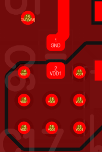
Stitching Vias
2. The Historical Evolution of Stitching Vias in PCB Manufacturing
The use of stitching vias in PCB manufacturing did not arise overnight. Like many innovations in electronics, their development was gradual—evolving in response to new technological challenges and opportunities. Tracing the historical context of stitching vias provides valuable perspective on how and why these design elements have become essential in modern circuit board fabrication.
From Simple Connections to Complex Systems
In the early days of PCB technology, the manufacturing focus was centered on simple signal routing and power delivery. Single-layer and later double-layer boards used basic through-hole vias to connect traces across layers. At this stage, the concept of via design was rudimentary, and all vias were treated equally—mere vertical wires enabling connectivity. There was little consideration for parasitic inductance, electromagnetic shielding, or thermal dynamics.
As multi-layer PCBs became more prevalent in the 1980s and 1990s, engineers began to encounter problems that stemmed from complex signal behavior. Signal integrity, crosstalk, and electromagnetic interference became significant design constraints, especially in telecommunications and computing applications. These challenges drove the demand for more sophisticated layer stack-ups, more rigorous ground referencing, and more refined via architectures.
The Birth of the Stitching Via Concept
The earliest references to what would become known as stitching vias appeared in high-speed PCB design literature in the early 1990s. Engineers experimenting with high-frequency signal paths began to notice that unbroken ground planes offered superior electromagnetic containment. However, when such ground planes were split by traces or cutouts, their shielding effectiveness degraded.
To address this, designers began placing multiple ground vias along board edges and around high-speed signal lines. These vias were not carrying signals themselves but instead acted as bridges, stitching together adjacent ground planes to maintain electrical continuity. Thus, the term “stitching via” was coined to describe this practice—akin to stitching fabric to reinforce its structure.
Adoption in RF and Microwave PCBs
By the late 1990s, stitching vias had found a permanent home in the design of RF and microwave PCBs. These systems operate in the GHz range and are especially sensitive to electromagnetic leakage, impedance mismatches, and parasitic coupling. Engineers learned that placing stitching vias around microstrip or stripline structures helped contain electromagnetic energy, improved return path quality, and stabilized signal performance.
In these applications, stitching vias began to appear in regular arrays—often forming vertical fences, edge barriers, or cavity walls. As CAD tools advanced, engineers could simulate the impact of via placement and density on electromagnetic behavior, making the design of stitching vias more deliberate and optimized.
Mainstream Integration and IPC Guidelines
In the 2000s and 2010s, the increasing speed of digital signals, driven by developments in CPUs, FPGAs, and high-speed interfaces (such as USB 3.0, PCIe, HDMI), led to a broader recognition of stitching vias beyond RF and microwave boards. Even in digital designs, ground integrity and EMI control became essential, and stitching vias emerged as a natural solution.
Organizations like IPC began incorporating recommendations for via spacing and placement into design standards, encouraging engineers to include stitching vias in multilayer designs and impedance-sensitive layouts. Design software such as Altium Designer, Cadence Allegro, and Mentor Graphics started offering automatic stitching via placement tools, reducing manual effort and standardizing practice.
Reflection: Engineering Evolution Through Subtle Innovation
It is fascinating how something as seemingly minor as a via—once merely a hole filled with copper—transformed into a strategic tool for thermal, mechanical, and electromagnetic performance. The evolution of stitching vias illustrates how innovation in engineering often emerges not from radical invention, but from careful observation, iterative improvement, and a willingness to challenge traditional assumptions.
As we continue through this article, we will see how stitching vias, though modest in appearance, represent a milestone in PCB design maturity—where engineers began to appreciate the hidden dimensions of system behavior and the invisible interactions that shape product reliability and performance.
3. Basic Concepts Behind Stitching Vias in PCB Manufacturing
To fully appreciate the importance of stitching vias in PCB manufacturing, it is essential to first understand their core functions and how they differ from other types of vias. This section unpacks the physical, electrical, and mechanical principles that make stitching vias an indispensable tool in modern circuit board design.
Definitions and Distinctions: What Are Stitching Vias?
At their core, vias are plated-through holes that allow electrical connections between different layers in a multilayer PCB. Vias typically fall into several categories based on their function:
-
Signal Vias – Transfer data or power between layers.
-
Thermal Vias – Facilitate heat dissipation across the board.
-
Blind/Buried Vias – Connect specific inner layers without going through the entire board.
-
Stitching Vias – Primarily used to connect ground planes or copper areas to maintain continuity, reduce impedance, and shield against electromagnetic interference (EMI).
Stitching vias, in particular, are distinguished not by their geometry but by their purpose and pattern. They are often placed in arrays or grids around sensitive areas—such as high-speed transmission lines, power planes, or shielding zones—creating low-inductance return paths and electrically “stitching” separate areas of the board together.
Electrical Function: Reducing EMI and Ground Bounce
One of the key electrical benefits of stitching vias is their ability to suppress unwanted electromagnetic emissions. In high-frequency designs, even short signal paths can radiate noise if the return path is discontinuous. Stitching vias help complete these return paths by providing a direct connection between ground planes, which are typically split or separated in multilayer stack-ups.
When placed correctly, stitching vias:
-
Minimize loop area, which directly reduces radiated emissions.
-
Improve signal integrity by preventing current from seeking unintended paths.
-
Reduce ground bounce, especially in densely populated or high-speed boards.
A small number of strategically positioned vias can make a substantial difference in EMI performance, reducing the need for external shielding and helping products meet electromagnetic compatibility (EMC) standards.
Mechanical Stability and Structural Integrity
Beyond their electrical role, stitching vias also enhance the mechanical resilience of PCBs. By tying multiple copper layers together, they:
-
Strengthen the board structure, especially in regions prone to flex or vibration.
-
Reduce the risk of delamination under thermal or mechanical stress.
-
Improve reliability in harsh environments, such as automotive or aerospace applications.
In flexible or rigid-flex boards, stitching vias may be arranged to provide both anchoring and expansion tolerance, preventing copper fracture or interlayer cracking.
Thermal Considerations
In designs involving power components or high thermal loads, stitching vias can double as thermal vias, helping conduct heat from surface-mounted devices into internal copper planes or to external heat sinks. While not as efficient as large-diameter thermal vias, a dense grid of stitching vias surrounding a power device can significantly reduce local temperatures and increase component lifespan.
This dual-role functionality—electrical and thermal—makes stitching vias especially valuable in compact, high-performance layouts where space and cooling options are limited.
Placement Strategies
The effectiveness of stitching vias depends heavily on their placement. Common strategies include:
-
Edge Stitching – Placing vias along the edge of ground planes or board boundaries to form EMI shields.
-
Via Fencing – Arranging vias in a row or grid parallel to high-speed signal lines to contain electromagnetic fields.
-
Component Shielding – Surrounding RF or sensitive analog components with a ring of vias to create a virtual Faraday cage.
-
Plane Coupling – Connecting isolated ground or power planes to maintain low-impedance continuity.
Best practices recommend placing vias as close as possible to the structures they are supporting—whether that’s a signal trace, a copper pour, or a component pad. The goal is always to shorten current paths, reduce impedance, and enforce symmetry.
Personal Reflection: The Elegance of Invisible Solutions
One reason stitching vias appeal to me personally is their subtlety. They do not attract attention like flashy components or advanced ICs. Yet, their presence often marks a board designed by someone who truly understands how electrons behave—not just in theory, but in the messy, imperfect reality of real-world hardware.
In a way, stitching vias are the engineers’ quiet protest against electromagnetic chaos. They offer elegant solutions to problems that only become visible in testing or field use. Their design requires forethought, precision, and a little humility—qualities that define good engineering.
4. Applications of Stitching Vias in PCB Manufacturing
The implementation of stitching vias spans a broad array of applications, driven by evolving demands in signal integrity, EMI suppression, thermal management, and mechanical strength. Their strategic value becomes evident when examining real-world use cases across various industries and PCB designs. This section explores where and how stitching vias are most effectively deployed in practical circuit board applications.
Stitching Vias in High-Speed Digital PCB Design
In modern high-speed digital circuits—such as those in computing, networking, and embedded systems—signal integrity is a top design priority. Interfaces like DDR, PCIe, HDMI, USB 3.x, and SerDes operate at frequencies where even minor layout irregularities can create serious problems.
Stitching vias are used here to:
-
Create continuous ground references for return currents alongside differential pairs.
-
Isolate high-speed lanes from noisy digital regions.
-
Minimize EMI by constructing stitching via fences near signal traces and return paths.
Designers often route high-speed traces over solid ground planes, placing stitching vias on both sides of the trace every quarter-wavelength to keep the impedance consistent. Without these vias, even well-matched differential traces may radiate noise or suffer from reflections due to improper ground continuity.
Stitching Vias in RF and Microwave Circuits
Perhaps the most classic and widespread use of stitching vias is found in RF and microwave PCB design. These circuits operate at frequencies from hundreds of MHz up to tens of GHz, where parasitic inductance and EMI must be tightly controlled.
In these contexts, stitching vias:
-
Create miniature Faraday cages around critical components and traces.
-
Provide grounding for coplanar waveguide or microstrip lines, ensuring minimal radiation.
-
Reinforce the electromagnetic boundary of shielded regions, reducing leakage and crosstalk.
A typical design might feature rows of stitching vias spaced closely around an RF path, forming what’s called a via fence. The spacing between vias is generally less than one-tenth of the operating wavelength to ensure effective shielding.
Stitching Vias in Multilayer Ground and Power Plane Integration
Multilayer PCBs often include multiple ground and power layers that need to be electrically consistent to maintain performance across the board. Stitching vias serve to:
-
Connect split ground regions to avoid floating or noisy ground islands.
-
Stabilize voltage reference planes by tying them to adjacent return planes.
-
Reduce impedance mismatches caused by layer transitions or segmentation.
A common example is a board where analog and digital circuits share a single PCB but require electrical isolation. Stitching vias are used to define “quiet zones” for analog signals while providing grounding points that suppress digital noise migration.
Stitching Vias in Shielding of Sensitive Analog Sections
Analog signal sections, particularly in applications like audio processing, sensor input, or analog front-ends (AFEs), are highly susceptible to interference from digital circuits. Stitching vias can be deployed as part of an EMI shielding wall, often surrounding:
-
Op-amp circuits
-
ADCs and DACs
-
Low-level sensor input circuits
They help to maintain consistent shielding when used alongside top-layer and bottom-layer copper pours. In designs where metal shields are added during assembly, stitching vias further enhance the effectiveness of the can by connecting it to internal ground layers.
Stitching Vias in Thermal Management Applications
When components dissipate significant heat—like power ICs, FETs, or LEDs—heat must be conducted away efficiently. Stitching vias arranged in a dense matrix beneath or around a hot component can conduct heat down to an internal ground or thermal plane, acting as a thermal via array.
Common applications include:
-
Power supply PCBs
-
LED driver boards
-
Motor driver circuits
-
RF power amplifiers
In such layouts, the stitching vias might not be primarily intended for EMI reduction but serve a vital thermal role while still contributing to ground plane connectivity.
Stitching Vias in EMI-Conscious Consumer Electronics
Smartphones, tablets, and laptops feature tightly packed PCBs with numerous high-frequency interconnects. In these designs, stitching vias help manage:
-
Antenna isolation
-
Internal EMI containment
-
Regulatory EMI compliance (FCC, CE, etc.)
Stitching via rings often form enclosures around shielded areas, reducing signal leakage and ensuring cleaner operation in proximity to antennas or other sensitive RF paths.
Stitching Vias in Automotive and Aerospace Systems
Automotive and aerospace PCBs operate in electrically and thermally harsh conditions. Stitching vias in these environments are not just for performance—they’re often crucial for safety, longevity, and compliance.
Applications include:
-
Reinforcing ground planes to prevent transient current loops
-
Reducing susceptibility to electromagnetic pulses (EMPs)
-
Providing thermal paths in high-power control units
In aerospace, where vibration is a serious concern, stitching vias can even enhance the mechanical bond between layers and reduce the chance of microcracks or interconnect failures under repeated stress.
Reflection: Versatility Rooted in Simplicity
What’s striking about the broad range of stitching via applications is how they fulfill so many critical roles—electrical, thermal, and mechanical—despite their small size and relative simplicity. They are among the most cost-effective design tools in a PCB engineer’s arsenal, offering performance gains without the need for expensive components or materials.
Their versatility makes them applicable in nearly every type of board, from consumer gadgets to life-critical avionics. Knowing where and how to use them effectively is a mark of both design experience and engineering foresight.
5. Design Guidelines for Stitching Vias in PCB Manufacturing
While stitching vias are conceptually straightforward, their effectiveness in practice hinges on thoughtful and precise implementation. Poor placement or incorrect design can negate their intended benefits or even introduce new problems. In this section, we explore practical design strategies, layout tips, and rules of thumb that help maximize the performance and reliability of stitching vias in modern PCB manufacturing.
Strategic Placement of Stitching Vias
The power of stitching vias lies not in their quantity, but in their strategic placement. Whether the design goal is EMI suppression, signal integrity, or thermal transfer, where vias are placed often matters more than how many are used.
Common placement strategies include:
-
Edge Stitching: Placing stitching vias along the perimeter of ground planes or copper pours to form a return path barrier or EMI shield.
-
Via Fences: Linear arrays of vias placed adjacent to high-speed signal lines to maintain continuous return paths and suppress radiation.
-
Enclosure Stitching: Surrounding sensitive areas or components (e.g., RF blocks, antennas, or analog ICs) to form an electromagnetic cage or isolate the zone from noisy neighbors.
-
Via-in-Pad Stitching: Integrating stitching vias directly within thermal or signal pads (used carefully to avoid solder wicking issues) for maximum connectivity and heat transfer.
These patterns ensure low-inductance paths and reinforce the local electromagnetic environment of critical zones on the board.
Stitching Via Dimensions: Diameter, Pad, and Spacing
To be effective, stitching vias must be dimensioned appropriately. Several physical parameters directly influence their electrical and thermal performance:
-
Hole Diameter: Typically ranges from 0.2 mm to 0.4 mm for standard stitching vias. Smaller diameters reduce board real estate but increase via impedance.
-
Pad Size: Usually 0.4 mm to 0.6 mm, ensuring a robust annular ring around the hole for good plating and manufacturing yield.
-
Via Spacing: Should be less than λ/10 at the highest frequency of interest for effective EMI shielding. In RF applications, this could mean placing stitching vias every 2–5 mm.
Too few stitching vias may cause discontinuities in the return path, while overly tight spacing might crowd the layout or raise manufacturing costs.
Layer Connectivity Considerations
Multilayer PCBs introduce complexity in how layers are interconnected. Designers must ensure stitching vias link the correct ground or power layers, not just blindly connect all metal layers.
Recommendations include:
-
Targeted Layer Connection: Use via stacks or via arrays to tie specific ground layers together (e.g., GND1 to GND2) to avoid unintended loops or noise propagation.
-
Anti-Pad Use: Place anti-pads (clearance holes) where vias must not connect to certain layers—preventing coupling to power planes or signal layers.
-
Split Plane Bridging: In boards with split ground planes (e.g., analog/digital), stitching vias placed at strategic crossover points can preserve signal return continuity without contaminating isolated grounds.
The goal is to create predictable and consistent return paths while respecting the electrical domain boundaries set in the stack-up.
Thermal Design Rules for Stitching Vias
When stitching vias are used for heat transfer in power or LED boards, thermal considerations become critical.
Design tips include:
-
Dense Grid Arrays: For heat-intensive components, use a matrix of stitching vias underneath the thermal pad or copper pour area.
-
Filled Vias: Consider filled or plugged vias with conductive epoxy or metal for superior thermal performance and reliability.
-
Copper Connection: Stitching vias must be tied to large copper areas (such as internal ground pours) to act as an effective heat sink.
-
Thermal Relief Patterns: Avoid thermal stubs or disconnected pours around stitching vias—ensure continuous copper connectivity to encourage thermal flow.
These tactics help spread and dissipate heat, reducing hot spots and protecting sensitive components from thermal stress.
DFM (Design for Manufacturability) Considerations
While effective, stitching vias can complicate the fabrication and assembly process if not designed with manufacturability in mind. Some critical DFM factors include:
-
Minimum Spacing: Respect the PCB manufacturer’s minimum via-to-via and via-to-trace spacing rules to prevent shorts or etching problems.
-
Via Tenting or Masking: Decide whether vias should be tented (covered with solder mask), open, or filled, based on the thermal and soldering needs.
-
Solder Wicking Prevention: When placing stitching vias in exposed thermal pads, consider using via-in-pad with filling and capping to prevent solder from draining during reflow.
-
Aspect Ratio Limits: Ensure the depth-to-diameter ratio of vias is within fabrication capabilities (usually ≤ 10:1) to ensure reliable plating.
Engaging with your PCB fabricator early in the design process is key to ensuring your stitching via design aligns with their capabilities.
Simulation and Analysis Before Fabrication
Simulation tools can model how stitching vias impact EMI, impedance, and heat dissipation before committing to a final layout. Modern EDA tools offer:
-
Return Path Visualization: To identify potential discontinuities and optimize via placement.
-
Electromagnetic Field Analysis: To assess shielding effectiveness of via fences and enclosures.
-
Thermal Simulation: To analyze heat flow through stitching vias and copper planes.
Simulation helps validate your layout assumptions and reduce design iterations, particularly in complex, high-frequency, or power-dense boards.
Personal Reflection: Art Meets Engineering
Designing effective stitching via layouts is part science, part art. On paper, the formulas and principles are well understood. But on the PCB layout canvas, engineers must make trade-offs between space, cost, signal paths, and manufacturing constraints.
What fascinates me most is how stitching vias, when designed carefully, become silent enablers of performance—hidden reinforcements that make the difference between a reliable board and one that fails under stress. Each via, though tiny, carries a purpose; together, they tell a story of foresight, discipline, and precision.
6. Challenges and Limitations of Stitching Vias in PCB Manufacturing
Despite their considerable benefits in high-speed, high-frequency, and thermally demanding PCB designs, stitching vias are not without challenges. Designers must navigate a variety of constraints—technical, spatial, and economic—to implement stitching vias effectively. This section explores the key limitations and practical obstacles associated with the use of stitching vias in PCB manufacturing.
Manufacturing Constraints of Stitching Vias
The fabrication process imposes several limits on how stitching vias can be designed and produced. These constraints affect not just the placement, but also the feasibility and cost of the entire PCB.
Key manufacturing constraints include:
-
Minimum Drill Size: PCB manufacturers typically limit via hole diameters to 0.2 mm or greater, depending on their capabilities. Using microvias for stitching may increase complexity and cost.
-
Aspect Ratio: The depth-to-diameter ratio must be manageable for proper plating. If stitching vias are too deep (in thick PCBs) or too narrow, reliable plating can become problematic.
-
Via Density and Spacing: Extremely dense arrays of stitching vias may require tighter manufacturing tolerances and increase the chance of shorts or incomplete etching between pads.
-
Drill Count and Cost: Stitching vias, especially in high quantities, add to the drill count, significantly influencing board cost and production time.
These limitations emphasize the need to balance via performance with manufacturing feasibility early in the design cycle.
Signal Integrity Risks Due to Improper Stitching Via Use
While intended to improve signal quality, poorly placed or incorrectly connected stitching vias can have the opposite effect—introducing discontinuities, reflections, or coupling paths.
Common risks include:
-
Interrupting Return Paths: If stitching vias do not provide a low-inductance path back to the signal’s reference plane, high-speed return currents may flow in unpredictable ways, radiating EMI or increasing crosstalk.
-
Stub Effects: Stitching vias that are unnecessarily tall (especially in multilayer PCBs) can behave like vertical stubs, introducing impedance discontinuities and potential resonances.
-
Excessive Parasitics: Every via introduces parasitic inductance and capacitance. Overusing stitching vias near sensitive nodes can degrade performance, especially in analog/RF designs.
In signal-critical applications, engineers must simulate and analyze stitching via effects to prevent such unintended consequences.
Space Consumption on Dense PCBs
PCB real estate is precious—especially in dense or miniaturized designs like smartphones, wearable devices, or compact RF modules. Stitching vias can consume a surprising amount of space when implemented extensively.
Trade-offs include:
-
Reduced Routing Channels: Every via takes up space on multiple layers, potentially blocking signal traces or requiring detours.
-
Obstacle to Plane Continuity: In densely packed power or ground planes, stitching vias may break up large copper areas if not designed with clearance or anti-pad strategies.
-
Component Placement Conflicts: Vias near components may interfere with solder mask openings or solder joint reliability, particularly in fine-pitch assemblies.
Designers must weigh the benefits of stitching against the cost of losing space or routing flexibility.
Thermal Expansion and Mechanical Stress Risks
In thermally active environments, stitching vias may become focal points of stress due to their copper content and vertical structure. This is particularly relevant in large PCBs, multilayer boards, or boards exposed to thermal cycling.
Issues that may arise include:
-
Via Cracking or Delamination: Repeated heating and cooling can cause micro-cracks in via barrels or pad delamination if the PCB material and via structure are mismatched.
-
CTE Mismatch: Differential expansion between copper (low coefficient of thermal expansion) and PCB substrate (higher CTE) can strain stitching vias over time.
-
Solder Joint Fatigue: Stitching vias placed too close to pads or thermal landings can distort solder flow and lead to joint fatigue, especially under vibration.
While not always critical, these risks should be considered in mission-critical or high-reliability designs (e.g., aerospace, automotive, or industrial controls).
Difficulty in Post-Manufacturing Rework
Once a PCB has been fabricated and assembled, modifying or correcting stitching via networks is often impractical or impossible.
Challenges include:
-
No Access for Probing: Stitching vias are often internal or covered by solder mask, making them inaccessible for in-circuit testing or probing.
-
Permanent Electrical Pathways: If vias were incorrectly connected (e.g., shorting analog and digital grounds), they cannot be cut or re-routed easily.
-
Limited Heat Application Area: Thermal stitching vias complicate rework around heat-sensitive components, as the copper connectivity disperses applied heat, making desoldering harder.
Thus, extensive simulation and review are vital before committing a stitching via design to production.
Cost Implications of Overuse
Although a single stitching via is inexpensive, the cumulative effect of using hundreds or thousands across a board can significantly affect cost, especially in mass production.
Cost drivers include:
-
Increased Drill Count: Every via requires machine time and tool wear, increasing fabrication cost.
-
Additional CAM Time: Complicated stitching patterns require more time for computer-aided manufacturing (CAM) processing.
-
Layer Stack Complexity: Stitching vias that span multiple layers might necessitate additional processing steps like sequential lamination or via filling.
-
Yield Risk: Higher via density increases the chance of manufacturing defects such as breakout or incomplete plating, reducing yield.
Designers must align their via strategy with the project’s cost and yield requirements to avoid overspending for marginal gains.
Personal Reflection: The Double-Edged Nature of Optimization
The challenges surrounding stitching vias underscore a broader engineering truth: every optimization comes at a cost. Stitching vias offer elegant solutions to problems of EMI, thermal resistance, and signal return—but they must be wielded with care. Over-designing is as dangerous as under-designing.
In my view, the most impressive PCB layouts are not those with the most vias, but those where each via serves a clear, validated purpose. The discipline to ask “why” before placing a via—and the humility to remove it if unnecessary—is what sets apart seasoned designers from the rest.
7. Innovations and Emerging Trends in Stitching Vias for PCB Manufacturing
As electronic systems evolve to support increasingly compact, high-speed, and power-intensive applications, stitching vias are also undergoing transformation. Emerging materials, advanced manufacturing techniques, and intelligent design automation are shaping how stitching vias are implemented in the next generation of PCBs. This section explores the forefront of technological innovation surrounding stitching vias in PCB manufacturing.
Advanced Microvia and HDI Integration for Stitching Vias
In the era of High-Density Interconnect (HDI) PCBs, traditional through-hole stitching vias are often too large and space-consuming. One of the most notable trends is the increasing use of microvias for stitching purposes.
Key innovations include:
-
Laser-Drilled Microvias: These allow for significantly smaller via diameters (down to 0.075 mm or less), ideal for fine-pitch components and tight spaces. Microvias can be stacked or staggered for more efficient vertical interconnects.
-
Sequential Lamination for HDI: Layer-by-layer construction enables designers to create stitching via networks that span only selected layers, reducing parasitic effects.
-
Copper-Filled or Conductive Paste Vias: Instead of traditional plating, microvias can be filled with solid copper or conductive resin, enhancing thermal and electrical continuity.
The shift toward microvia-based stitching via strategies supports more compact and higher-frequency designs while preserving signal integrity and EMI suppression.
Automated Stitching Via Optimization Tools
As design complexity increases, engineers are turning to intelligent design automation tools to optimize the placement and quantity of stitching vias. These tools integrate with PCB design software and rely on algorithms to meet electromagnetic and thermal constraints efficiently.
Emerging capabilities include:
-
EMI-aware Via Placement Engines: These analyze board layout in real time and suggest via positions to minimize loop areas or maximize shielding efficiency.
-
Thermal Mapping Tools: Designers can simulate heat flow across power planes and automatically populate stitching vias in high-dissipation regions.
-
Return Path Optimization Algorithms: Signal integrity tools can recommend stitching via positions along high-speed signal paths to ensure low-impedance return loops.
These automated methods improve design accuracy, reduce time-to-market, and eliminate overdesign—especially in complex multilayer PCBs.
Use of Stitching Vias in Flexible and Rigid-Flex PCBs
As flexible electronics continue to gain ground in wearables, automotive, and medical devices, stitching vias are being adapted to non-traditional substrates.
Key developments:
-
Stitching Vias in Rigid-Flex Boards: Vias placed between rigid sections and flex zones help manage EMI across bending regions, often with mechanically reinforced structures to maintain reliability.
-
Flexible Via Structures: Some designs now use reinforced polyimide or embedded conductors to mimic the functionality of stitching vias without physical drilling, improving flexibility.
-
Dynamic Thermal Pathways: In high-heat flex circuits (e.g., LED lighting), stitching vias are distributed along bendable zones to dissipate heat without compromising mechanical durability.
The challenge is maintaining reliability in flexible environments without the traditional rigidity that helps support via structures.
Additive Manufacturing Techniques for Stitching Vias
The use of additive manufacturing, such as 3D printing, in PCB fabrication introduces new opportunities for embedding and forming stitching vias in unconventional ways.
Innovative methods include:
-
Printed Conductive Inks: Stitching vias can be formed by printing conductive materials directly into via channels or onto surfaces, skipping conventional plating processes.
-
Laser Sintering of Metals: Direct sintering of metal nanoparticles using lasers enables the creation of high-density interconnects including stitching vias at very small scales.
-
Multi-material Layer Deposition: Some advanced 3D PCB printers can simultaneously lay down dielectric and conductive layers, forming vias as part of the printing process.
Although still in experimental or low-volume stages, these approaches promise faster prototyping, reduced tooling costs, and greater design flexibility.
Integration of AI in Stitching Via Decision-Making
Artificial intelligence is beginning to assist with design intelligence, particularly in optimizing stitching via networks in complex designs.
AI applications include:
-
Pattern Recognition from Legacy Boards: AI systems can analyze past designs and identify optimal via patterns for similar use cases, reducing the need for manual placement.
-
Predictive Failure Modeling: AI can model the likelihood of thermal or mechanical failure based on via arrangements, guiding designers to more robust configurations.
-
Generative Layout Algorithms: AI-powered layout tools are now capable of producing via placement strategies based on user-defined goals like EMI reduction or layer density constraints.
These technologies improve accuracy and free engineers from repetitive tasks, allowing them to focus on system-level thinking.
Environmental and Sustainability Considerations
Sustainability is influencing how stitching vias are produced and designed, as manufacturers and customers push for greener electronics.
Emerging trends:
-
Material Reduction: Designs now strive to reduce copper usage without sacrificing performance by using simulation-driven placement of minimal via arrays.
-
Low-Energy Processing Techniques: Methods such as photo-defined vias and low-temperature plating help reduce energy consumption and chemical waste.
-
Recyclability-Oriented Design: In some high-volume consumer electronics, vias and board stack-ups are optimized to facilitate future recycling and minimize toxic material usage.
While stitching vias are a small part of a board, their design and quantity can significantly influence overall sustainability when scaled to millions of units.
Personal Reflection: Embracing a Future-Driven Mindset in PCB Design
The innovations around stitching vias are a reminder that even the most basic elements of circuit design are not static. Vias, once thought of as passive, are now evolving through AI, additive manufacturing, and advanced materials. As designers, we must cultivate a mindset that anticipates future possibilities rather than clings to past practices.
In my opinion, embracing emerging via strategies isn’t just about performance or miniaturization—it’s about unlocking new freedoms in design thinking. The more we understand the capabilities of stitching vias, the more power we have to shape the functionality, form, and environmental footprint of our electronic systems.
8. Design Guidelines and Best Practices for Stitching Vias in PCB Manufacturing
The successful implementation of stitching vias in PCB manufacturing depends not only on understanding their theoretical benefits but also on adhering to practical design rules. A well-engineered via network ensures optimal signal performance, mechanical reliability, and manufacturability. This section explores key guidelines, common pitfalls, and best practices to follow when incorporating stitching vias into your PCB designs.
Stitching Vias Spacing and Placement Guidelines
Effective spacing and placement are crucial to achieving the desired benefits from stitching vias, whether for EMI shielding, signal integrity, or thermal control.
Key guidelines:
-
Perimeter Stitching: For ground planes around high-speed signal layers or power islands, stitching vias should be placed approximately every 0.2–0.3 λ (wavelength) of the highest frequency of interest.
-
Shielding Walls: For sensitive analog or RF components, lines of stitching vias can form effective shielding walls. Vias should be spaced no more than 1/20th of the signal wavelength.
-
Return Path Optimization: Place stitching vias close to the signal via or trace (within 3 mm) to ensure a low-impedance return path, particularly near layer transitions.
-
Thermal Distribution: When managing heat, distribute vias evenly across copper zones to prevent hot spots and thermal gradients.
Well-placed stitching vias not only improve EMI suppression but also prevent return current detours that can introduce delay or noise.
Stitching Vias Size and Aspect Ratio Considerations
While stitching vias typically use standard mechanical drilling, the choice of via size and the aspect ratio (board thickness to hole diameter) can significantly affect performance and reliability.
Best practices include:
-
Hole Size: Common diameters for stitching vias range from 0.3 mm to 0.5 mm. For high-density areas, smaller microvias (down to 0.1 mm) may be used.
-
Aspect Ratio: Aim for an aspect ratio less than 10:1 to ensure good plating quality and avoid barrel cracking. For thicker boards, consider larger diameters or via-in-pad designs.
-
Pad and Antipad Dimensions: Ensure adequate clearance around vias, especially in power or ground layers, to prevent accidental shorts or impedance mismatches.
Adhering to recommended aspect ratios ensures long-term durability and minimizes failure during reflow or thermal cycling.
Layer Stackup and Stitching Vias Integration
The layer stackup design plays a central role in how stitching vias interact with signals and planes across the PCB.
Guidelines:
-
Plane Pairing: Pair signal layers with ground or power planes for effective return paths and EMI control. Stitching vias must bridge these planes to preserve continuity.
-
Blind/Buried Vias: Use blind or buried stitching vias to reduce surface crowding in dense HDI designs while still ensuring electromagnetic performance.
-
Via Transitions: In multi-layer boards, place stitching vias at layer transition points for differential pairs or clock signals to reduce mode conversion and reflection.
Strategically integrating vias into the stackup prevents parasitic effects and supports high-speed signal routing.
Thermal and Mechanical Reliability Considerations for Stitching Vias
Stitching vias must remain reliable through environmental stresses like heating, vibration, and mechanical flexing—especially in automotive, aerospace, or wearable applications.
Key considerations:
-
Copper Plating Thickness: Ensure via barrels have at least 20 µm of copper plating to withstand thermal expansion.
-
Resin-Filled or Capped Vias: In applications requiring via-in-pad structures or mechanical support, resin filling enhances reliability and prevents solder wicking.
-
Via Tent or Masking: Covering via tops with solder mask prevents moisture ingress and oxidation, particularly for external stitching vias.
-
Vibration Resistance: Distribute stitching vias uniformly in areas subject to shock or movement to reduce stress concentration.
These mechanical guidelines protect against via cracking and intermittent connectivity failures over the product’s lifespan.
Stitching Vias in High-Frequency and RF Applications
High-frequency PCBs demand precision when incorporating stitching vias to prevent signal degradation, crosstalk, and radiation.
Best practices for RF use:
-
Reference Plane Matching: Stitching vias must tightly connect all ground reference planes to ensure consistent impedance and prevent unintended signal loops.
-
Via Fencing: Place stitching vias in rows or fences around transmission lines (e.g., microstrip, stripline) to confine electric fields and reduce EMI.
-
Differential Pair Guarding: For differential pairs, align stitching vias symmetrically on both sides of the pair to preserve balance and reduce common-mode noise.
-
Simulation Validation: Always run electromagnetic simulation tools to model the effect of via placement, especially in GHz-range designs.
In RF contexts, precision is paramount—small changes in stitching via layout can make or break performance.
Common Mistakes to Avoid with Stitching Vias
Even experienced designers can fall into traps that compromise the effectiveness of stitching vias.
Avoid these pitfalls:
-
Overuse Without Purpose: Excessive vias increase drilling cost and may degrade signal performance by adding unnecessary parasitics.
-
Misaligned Vias on Split Planes: Stitching vias on split ground or power planes can cause return path disruption and induce noise.
-
Ignoring Manufacturing Limits: Placing vias too close to edges, pads, or each other can result in poor plating, shorting, or manufacturing failure.
-
Neglecting Return Paths: Adding stitching vias far from critical signal transitions can nullify their intended benefit.
Designing with intention and discipline ensures stitching vias serve their function rather than interfere.
Personal Reflection: Balancing Functionality with Manufacturability
From my own design experience, mastering stitching vias is about finding balance. It’s tempting to think more vias mean better performance, but thoughtful placement, aligned with simulation and empirical data, almost always yields superior outcomes. Working closely with fabrication partners early in the design process can also prevent surprises during prototyping.
Good design isn’t just about performance—it’s about manufacturability, cost-effectiveness, and long-term reliability. Stitching vias exemplify this harmony, where electrical, mechanical, and production disciplines converge.
9. Future Trends and Innovations in Stitching Vias for PCB Manufacturing
As printed circuit board (PCB) technology continues to advance rapidly, the role of stitching vias evolves in parallel, adapting to new challenges and unlocking novel possibilities. This section explores emerging trends, cutting-edge innovations, and future directions that are shaping how stitching vias will be designed and utilized in next-generation PCB manufacturing.
Integration of Advanced Materials in Stitching Vias
With the drive for higher performance and miniaturization, materials used in stitching vias are undergoing innovation.
-
Copper Alternatives and Coatings:
Research into alternative conductive materials such as graphene or silver-based plating aims to improve conductivity and reduce via resistance, especially in high-frequency or high-current applications. Additionally, new anti-oxidation coatings promise longer reliability and less signal degradation. -
Embedded Via Filling Materials:
The use of resin-filled or conductive polymer-filled stitching vias is increasing, offering improved mechanical strength and thermal conductivity while preventing solder wicking. This is especially important for via-in-pad designs on high-density PCBs.
Advancements in Via Fabrication Techniques
Emerging fabrication methods are improving stitching via quality, precision, and density:
-
Laser Drilling and Microvias:
Laser drilling technology enables the creation of smaller, more precise stitching vias with aspect ratios previously unattainable. This supports ultra-high-density interconnect (HDI) boards where space is at a premium. -
Additive Manufacturing:
Emerging additive processes like inkjet or aerosol jet printing for conductive vias may reduce production steps and enable novel via geometries that enhance stitching performance. -
Via-in-Pad Technology Enhancements:
Integration of stitching-vias directly into component pads reduces parasitic inductance and improves signal return paths, critical in RF and high-speed digital designs.
Simulation-Driven Stitching Via Design
Simulation tools are becoming more sophisticated, allowing engineers to model stitching-via behavior with unprecedented accuracy:
-
Electromagnetic Field Simulation:
Tools can simulate EMI shielding effects of stitching-vias, optimizing spacing and patterns before fabrication to minimize trial and error. -
Thermal and Mechanical Stress Analysis:
Advanced finite element analysis (FEA) helps predict thermal gradients and mechanical stresses on stitching vias, enabling designs that improve reliability in harsh environments. -
AI and Machine Learning:
AI-driven design assistants can suggest optimal stitching via layouts based on board function, reducing design time and improving performance.
Multi-Functional Stitching Vias
Future stitching-vias are envisioned not just as passive electrical connectors but multifunctional elements:
-
Embedded Sensors and Monitoring:
Stitching vias could incorporate embedded sensors for temperature, humidity, or strain, enabling real-time health monitoring of PCBs. -
Integrated Cooling Channels:
Hybrid vias combining electrical conduction with microfluidic cooling pathways are being researched to address thermal challenges in high-power electronics. -
Signal Conditioning Elements:
Incorporation of thin-film resistors or capacitors in via structures to improve signal integrity and filtering without increasing board size.
Sustainability and Cost-Effectiveness
With increasing environmental awareness, innovations in stitching-vias also focus on sustainability:
-
Material Recycling:
Development of PCB designs that enable easier recovery and recycling of via materials to reduce e-waste. -
Eco-Friendly Manufacturing Processes:
Reducing chemical use and energy consumption in via drilling and plating steps while maintaining quality. -
Design for Manufacturability:
Creating stitching-via strategies that minimize board complexity and drilling time, lowering costs without compromising performance.
Industry Trends Influencing Stitching Via Development
The following broader industry trends will continue to impact stitching via technology:
-
5G and Beyond:
Ultra-high-frequency applications require even more precise stitching via placement to manage complex electromagnetic environments. -
Automotive Electrification:
Electric vehicles (EVs) and autonomous driving systems demand PCBs with robust thermal and EMI control, elevating stitching-via importance. -
Wearable and Flexible Electronics:
Flexible PCBs need stitching-vias that maintain connectivity under bending and flexing stresses, driving innovations in via materials and mechanical design.
Personal Insight: Preparing for the Next Era of PCB Design
Reflecting on the rapid pace of PCB technology, the future of stitching-vias lies at the intersection of materials science, precision manufacturing, and smart design tools. Designers must stay adaptable—learning to harness new fabrication methods and simulation capabilities while balancing cost and sustainability.
I believe that stitching-vias will transition from traditional “fixes” to strategic enablers of novel PCB functions, making them indispensable in advanced electronics across industries. Embracing these innovations early will give engineers a competitive edge in delivering cutting-edge, reliable, and sustainable PCBs.
10. Conclusion on the Uses of Stitching Vias in PCB Manufacturing
Stitching-vias have firmly established themselves as a fundamental element in modern PCB design and manufacturing. This article has explored their multifaceted roles—from improving electromagnetic compatibility and signal integrity to enhancing thermal management and mechanical robustness. As we’ve seen through detailed analysis and case studies, stitching-vias contribute critically to the performance and reliability of a wide range of PCB applications.

- long board pcb
- Flexible PCBs
- Special PCB
- Express Printed Circuit Board
- Pcb Prototype
- LED PCB
- PCB
- Printed Circuit Board
- Pcb meaning
- Pcb manufacturer
- Rigid pcb board
- Rigid Flex PCB
 Quote
Quote
 E-mail