Stack Up in PCB Manufacturing
Introduction
Stack up is a critical stage in multilayer PCB (printed circuit board) manufacturing where the individual inner layers are carefully stacked and prepared for the lamination process. This step ensures that the layers are properly aligned, free from contamination, and securely positioned to achieve a high-quality laminated structure.
As PCB designs become more complex with higher layer counts, finer traces, and stricter tolerances, the importance of a well-executed stack up has increased significantly. Any misalignment or contamination during this phase can lead to defects such as delamination, registration errors, and poor electrical performance. This article will explore the purpose, key processes, equipment, quality control measures, and challenges associated with stack up in PCB manufacturing.
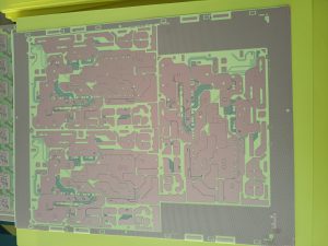
Stack Up Before Lamination
Purpose of Stack Up
The main objectives of stack up include:
- Ensuring Precise Layer Alignment – Accurate alignment of inner layers prevents registration errors and enhances PCB performance.
- Minimizing Contaminants – Prevents dust, debris, and moisture from being trapped between layers.
- Maintaining Structural Integrity – Ensures proper positioning of layers before the high-pressure lamination process.
- Enhancing Bonding Strength – Prepares surfaces for strong adhesion during lamination.
- Preventing Air Pockets and Voids – Helps to eliminate trapped air, reducing the risk of defects.
Proper execution of stack up ensures that the final PCB meets industry standards and functional requirements.
Key Processes in Stack Up
Stack up involves several precise steps to ensure alignment, cleanliness, and secure positioning of PCB layers before lamination.
1. Inner Layer Inspection and Cleaning
- Objective: Remove any contamination, oxidation, or debris from the copper surfaces of inner layers.
- Methods Used:
- Chemical cleaning
- Mechanical brushing
- High-pressure air blowing
- Outcome: A contaminant-free surface that enhances adhesion between layers.
2. Alignment and Layer Registration
- Objective: Precisely align all PCB layers to prevent misregistration and electrical shorts.
- Methods Used:
- Optical alignment systems for precision positioning
- Pin tooling systems to maintain correct layer order
- Automated layer stacking equipment for high-accuracy alignment
- Outcome: Consistently positioned layers, ensuring proper circuit connectivity.
3. Pre-Bonding (Tacking or Pre-Tacking)
- Objective: Securely hold the stacked layers together before lamination.
- Methods Used:
- Vacuum tack welding
- Pre-tack bonding adhesives
- Pressure clamping techniques
- Outcome: A stable multilayer stack ready for the lamination process.
4. Prepreg Placement
- Objective: Distribute prepreg (bonding resin sheets) between the copper layers to act as an adhesive during lamination.
- Considerations:
- Ensure uniform prepreg thickness to avoid uneven bonding.
- Use precisely cut prepreg sheets to match PCB dimensions.
- Outcome: Well-positioned prepreg layers ensuring strong and void-free lamination.
5. Layer Securing (Tack Welding or Tape Fixation)
- Objective: Prevent shifting of layers before final lamination.
- Methods Used:
- Tack welding with heat to hold layers temporarily
- Adhesive tape or clamps to stabilize stack-up
- Outcome: Secure layer positioning without movement during transfer to the laminating press.
Equipment Used in Stack Up
Various machines and tools are used to enhance precision and efficiency in stack up, including:
- Automatic Optical Alignment Machines – Ensures high-precision registration of PCB layers.
- Vacuum Cleaning Systems – Removes particles and dust to prevent contamination.
- Layer Stacking Systems – Uses automated handling to position layers with extreme accuracy.
- Pre-Bonding Press Machines – Applies low-pressure heat bonding to secure the stacked layers.
- Pin Tooling Fixtures – Provides mechanical alignment for manual or automated layer positioning.
- Environmental Control Chambers – Maintains optimal humidity and temperature to prevent moisture absorption.
Quality Control Measures
To ensure high reliability and precision, manufacturers implement strict quality control checks during the stack up phase.
1. Alignment and Registration Inspection
- Purpose: Verifies that all layers are accurately aligned before lamination.
- Methods:
- Automated optical inspection (AOI)
- X-ray imaging for internal layers
- Tolerance Requirement: Typically ±25μm for fine-line PCBs.
2. Surface Cleanliness Testing
- Purpose: Ensures that layers are free of dust, moisture, and contaminants.
- Methods:
- Microscopic analysis for residue detection
- Ion chromatography for chemical contamination analysis
3. Prepreg Thickness Verification
- Purpose: Ensures consistent resin flow and uniform bonding strength.
- Methods:
- Digital micrometers for measuring prepreg thickness
- Dielectric measurement techniques
4. Layer Bonding Strength Testing
- Purpose: Confirms that pre-bonding is sufficient to hold layers in place.
- Methods:
- Peel strength tests
- Shear stress testing
Common Challenges and Solutions in Stack Up
1. Misalignment Between Layers
- Cause: Poor registration during stacking.
- Solution: Use high-precision optical alignment systems.
2. Contamination Issues
- Cause: Dust, fingerprints, or oxidation on copper layers.
- Solution: Implement strict cleaning protocols and anti-static control.
3. Layer Shifting During Handling
- Cause: Improper fixation of layers.
- Solution: Use tack welding or precise tape fixation methods.
4. Uneven Prepreg Distribution
- Cause: Incorrect prepreg cutting or improper placement.
- Solution: Automate prepreg positioning and use thickness verification tools.
Conclusion
Stack up is a crucial step in PCB manufacturing, ensuring proper layer alignment, contamination control, and bonding stability before final lamination. By optimizing alignment techniques, using high-precision equipment, and implementing rigorous quality control, manufacturers can achieve higher yields, reduced defects, and improved PCB reliability.
As PCB designs continue to evolve with higher layer counts and finer traces, advancements in automated stacking, optical alignment, and contamination prevention will further enhance the stack up process, ensuring superior performance and long-term reliability in modern electronic applications.
our linkedin sqpcb.com

- long board pcb
- Flexible PCBs
- Special PCB
- Express Printed Circuit Board
- Pcb Prototype
- LED PCB
- PCB
- Printed Circuit Board
- Pcb meaning
- Pcb manufacturer
- Rigid pcb board
- Rigid Flex PCB
 Quote
Quote
 E-mail