Solder mask defined (SMD) pads and non-solder mask defined (NSMD) pads are critical in modern PCB design, especially for high-density and fine-pitch components like BGAs. Understanding their differences and proper application ensures better soldering quality and enhanced reliability in electronic devices. This article provides a detailed guide to SMD and NSMD pads, their characteristics, design principles, and best practices.
Solder mask defined pads
What Are Solder Mask Defined (SMD) Pads?
Solder mask defined pads use solder mask material to define the size of the solder pad by covering the surrounding copper. The solder mask opening is smaller than the copper pad, exposing only the required area for soldering.
Key Features of SMD Pads
-
-
Improved Pad Stability: The solder mask helps anchor the pad to the PCB substrate, providing better mechanical strength.
-
Smaller Solder Area: The solder area is more controlled, limiting the spread of solder and making it ideal for fine-pitch components.
-
Applications: SMD pads are most commonly used in BGAs, CSPs (Chip Scale Packages), and other high-density designs where precise soldering is critical.
-
Solder mask defined pads provide a more controlled approach to soldering, reducing the risk of bridging and ensuring greater precision in designs. SQPCB ensures top-notch quality for these types of pads, offering tailored solutions for high-precision applications and quick-turn prototyping.
What Are Non-Solder Mask Defined (NSMD) Pads?
In contrast to SMD pads, non-solder mask defined (NSMD) pads leave the entire copper pad exposed for soldering. The copper pad size is smaller than the solder mask opening, providing greater flexibility in layout and routing.
Key Features of NSMD Pads
-
-
Larger Solder Area: With exposed copper, solder can adhere to both the top and sides of the pad, resulting in stronger solder joints.
-
Greater Design Flexibility: Smaller pads allow for easier routing, especially in high-density layouts like BGAs.
-
Applications: NSMD pads are ideal for designs that require robust solder joints, such as power electronics, RF designs, and situations where reliability is paramount.
-
NSMD pads are best suited for applications that demand superior joint strength and better routing flexibility, making them ideal for more complex PCB layouts.
SMD vs. NSMD Pads: Key Differences
| Aspect | SMD Pads | NSMD Pads |
|---|---|---|
| Solder Mask Opening | Smaller than the copper pad | Larger than the copper pad |
| Solder Joint Area | Limited to the exposed copper pad surface | Includes both the surface and sides of the pad |
| Pad Stability | More stable due to solder mask support | Less stable, more prone to detachment |
| Routing Flexibility | Limited due to larger pad size | Easier due to smaller pad size |
| Applications | High-density, fine-pitch components (e.g., BGAs) | Designs needing stronger solder joints |
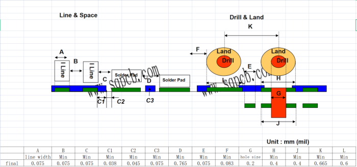
Design Principles for Solder Mask Defined Pads
- Pad Size
- Ensure the pad’s minimum side width is at least 0.25 mm, and its diameter does not exceed three times the device aperture. This ensures good solderability and mechanical strength.
- Solder Mask Openings
- The solder mask opening should be slightly larger than the copper pad for NSMD designs (typically by 0.1 mm) to prevent oxidation and ensure proper soldering.
- Pad Spacing
- Maintain a minimum spacing of 0.4 mm between adjacent pads to avoid solder bridging or short circuits, especially in high-density layouts.
- Pad Shapes
- Use round, square, or oval pads depending on the component type. Shape uniformity is critical for maintaining consistent soldering quality.
- Solder Mask Role
- Ensure the solder mask accurately covers areas outside the pad to prevent unwanted soldering and oxidation while enhancing mechanical stability.
- Pad Uniformity
- Maintain consistent pad size and shape across the design to ensure uniform soldering and avoid process variations.
Advantages of SMD and NSMD Pads
SMD Pads
-
-
Higher Stability: Stronger bonding between the pad and PCB substrate due to solder mask support.
-
Ideal for High-Density Applications: Minimizes soldering issues, especially in compact layouts like those used in BGAs.
-
NSMD Pads
-
-
Better Solder Joint Strength: Larger soldering area increases joint strength, especially in power and high-current applications.
-
Greater Routing Flexibility: Smaller pads provide better flexibility for routing, especially in complex designs with dense component placement.
-
Best Practices for SMD and NSMD Pad Design
1. Match the Pad Type to the Application
Use SMD pads for fine-pitch components like BGAs. For applications requiring robust solder joints or complex routing, NSMD pads are a better choice.
2. Ensure Accurate Fabrication
Collaborate with your PCB manufacturer to verify pad dimensions, solder mask alignment, and process tolerances. Manufacturers like SQPCB ensure that pad fabrication and mask alignment are precise, minimizing errors during production.
3. Test Soldering Performance
Regularly inspect solder joints during prototyping to ensure your design meets the required functionality and performance standards. Always test the design to avoid potential issues in mass production.
Conclusion
Solder mask defined (SMD) and non-solder mask defined (NSMD) pads are essential components in PCB design. Each offers unique advantages depending on the application, with SMD pads providing higher stability and NSMD pads allowing for better solder joint strength and routing flexibility. By understanding their differences and applying the correct design principles, engineers can optimize the soldering quality and performance of their PCB board.
Whether you’re designing high-density BGAs or high-power applications, selecting the right pad type is critical for reliable and efficient circuit boards. For precision-engineered solutions, SQPCB provides custom PCB manufacturing with tailored SMD and NSMD pad designs to meet your exact needs.
Frequently Asked Questions (FAQ)
Q1: When should I use SMD pads over NSMD pads?
A1: Use SMD pads for fine-pitch components like BGAs, where space is limited and precise soldering is required. NSMD pads are better for applications needing stronger solder joints and higher-density routing.
Q2: What is the recommended pad size for high-density designs?
A2: For high-density designs, ensure the pad size is appropriate for the component pitch. The minimum pad size for SMD designs is typically 0.25 mm, while for NSMD pads, careful consideration of spacing is required to avoid short circuits.
Q3: Can I use NSMD pads for power components?
A3: Yes, NSMD pads are ideal for power components where a stronger solder joint is required. The larger soldering area provides better adhesion and mechanical stability.
Q4: How does solder mask affect PCB reliability?
A4: The solder mask ensures that pads are protected from oxidation and contaminants, which improves solder joint reliability. For SMD pads, the solder mask also adds mechanical support, ensuring a stronger connection.
Q5: How can I ensure the accuracy of my PCB design?
A5: Collaborate with an experienced manufacturer like SQPCB to verify pad dimensions, solder mask alignment, and overall design. They provide design-for-manufacturing (DFM) feedback to ensure your pads meet tolerance requirements for mass PCB production.

- long board pcb
- Flexible PCBs
- Special PCB
- Express Printed Circuit Board
- Pcb Prototype
- LED PCB
- PCB
- Printed Circuit Board
- Pcb meaning
- Pcb manufacturer
- Rigid pcb board
- Rigid Flex PCB
 Quote
Quote
 E-mail