1. Introduction to Resistance and Current in Circuit Design
Circuit design is at its core an exercise in controlling electrical flow. To control flow, engineers must deeply understand two interdependent concepts: resistance and current. The way resistance influences current, and in turn how current behaves when it encounters varying resistance, is the foundation of every reliable and high-performing circuit board. Without a solid grasp of this relationship, even the most sophisticated design tools cannot guarantee stability, efficiency, or longevity.
At a high level, current is the movement of charge through a conductor, while resistance is the opposition that restricts that movement. Ohm’s law, the simple yet profound equation V = IR, captures this relationship. But in real-world electronics, especially in PCB design, the dynamics go beyond the textbook definition. Resistance is not merely a static property—it varies with temperature, material type, and frequency. Likewise, current can fluctuate depending on load, supply characteristics, and environmental conditions.
I believe the true mastery of circuit design lies in anticipating how these fluctuations interact. In this sense, mastering flow is not just about calculation—it is about foresight and engineering intuition.
resistance and current
2. The Scientific Foundations of Resistance and Current
When explaining resistance and current, it is tempting to rely only on mathematical expressions. However, the science involves material physics, electron mobility, and even quantum mechanics in certain extreme cases.
2.1 Defining Resistance and Current in Physical Terms
-
Current (I): The rate at which electrons pass through a cross-section of conductor. Its unit, the ampere (A), corresponds to one coulomb of charge per second.
-
Resistance (R): The measure of how much a material resists current flow. It depends on material resistivity (ρ), length (L), and cross-sectional area (A): R=ρ (A/L)
3. Practical Applications of Resistance and Current in Modern Circuits
Understanding resistance and current is not limited to academic knowledge—it translates directly into practical engineering.
3.1 Resistance and Current in Power Distribution Networks
Power rails in a PCB are designed to carry currents without significant voltage drop. Resistance of copper traces must be minimized; otherwise, devices receive less voltage than intended. Engineers calculate width and thickness to balance manufacturability with performance.
3.2 Resistance and Current in Signal Integrity
For high-speed digital circuits, resistance plays a role in impedance control. If resistance mismatches occur, reflections can corrupt data transmission. Here, resistance and current dynamics are coupled with capacitance and inductance, creating a delicate balance.
3.3 Resistance and Current in Thermal Management
Current flowing through resistance produces heat (Joule heating). This is why thermal vias, copper planes, and heat sinks are integrated into PCBs. Without managing this effect, circuit boards overheat, leading to failure.
4. The Advantages of Understanding Resistance and Current for Engineers
There are many advantages of mastering resistance and current as core design principles:
-
Efficiency Improvement: Proper resistance design reduces energy wasted as heat.
-
Reliability: Balanced current distribution prevents hotspots and premature component failure.
-
Performance Optimization: Impedance matching ensures faster and cleaner data transmission.
-
Cost Reduction: Avoiding overdesign (excessive copper thickness or unnecessary components) saves material costs.
In my personal observation, engineers who view resistance and current holistically—rather than as isolated calculations—tend to produce designs that withstand real-world conditions better.
5. Resistance and Current in PCB Design and Their Performance Impact
Nowhere is the impact of resistance and current more visible than in PCB design.
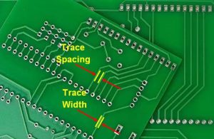
5.1 Trace Geometry and Resistance and Current
Wider and thicker copper traces reduce resistance, allowing larger currents with less heating. Narrow traces, often used in compact designs, must be carefully engineered to avoid overheating.
5.2 Via Design and Resistance and Current
Every via introduces some resistance. In high-current applications, multiple vias in parallel are recommended to prevent localized heating.
5.3 Material Selection and Resistance and Current
FR-4, polyimide, and advanced laminates differ in thermal conductivity and dielectric properties. These materials influence how current interacts with resistance at different frequencies.
6. Resistance and Current in High-Frequency and High-Speed Systems
High-speed and RF circuits bring new challenges. At gigahertz frequencies, resistance is frequency-dependent due to the skin effect, where current flows primarily on the conductor’s surface. Engineers must therefore consider both AC resistance and DC resistance in calculations.
Misjudging this effect can ruin an otherwise well-designed RF circuit. I personally believe this is one of the most overlooked areas in circuit design by entry-level engineers, who often rely on DC approximations only.
7. Resistance and Current in Power Electronics and Energy Systems
Power electronics operates at the intersection of high voltage, high current, and strict efficiency demands. In this field, resistance and current management is more than a design choice—it is the difference between success and catastrophic failure.
7.1 Resistance and Current in Power Conversion
Power converters (AC-DC or DC-DC) must ensure that current flows through switching devices and inductors with minimal resistive losses. The wrong choice of copper trace thickness can raise resistive heating, wasting power and decreasing efficiency.
For example, in a buck converter, even milliohms of extra resistance in a high-current path can reduce conversion efficiency significantly. At scale—say, in server farms—these small losses accumulate into large costs.
7.2 Resistance and Current in Renewable Energy Systems
Solar inverters, wind turbine converters, and battery management systems are highly sensitive to resistance and current dynamics. Panels may output hundreds of amps; hence PCB busbars and heavy copper designs must be optimized to prevent overheating.
I personally view this as an area where younger engineers sometimes under-appreciate real-world losses. They may focus on ideal equations, but in reality, parasitic resistance in long PCB traces can degrade system output by measurable percentages.
7.3 Safety Implications of Resistance and Current
In high-power systems, excess current through a resistive trace can cause arc faults or even fire. Fuses, current sensors, and intelligent monitoring are therefore integrated. A holistic understanding of resistance and current ensures both performance and safety.
8. Resistance and Current in Analog vs. Digital Circuit Architectures
Analog and digital circuits respond differently to the interplay of resistance and current.
8.1 Resistance and Current in Analog Circuits
Analog designs—such as amplifiers, filters, and oscillators—are highly sensitive to resistance values. Current flow must be stable; otherwise, noise and distortion increase.
Take an audio amplifier: mismatched resistance can raise the noise floor, reducing clarity. A carefully chosen resistor network not only sets gain but also stabilizes current through transistors.
8.2 Resistance and Current in Digital Circuits
Digital logic, by contrast, operates in binary states, but resistance and current still matter. For instance:
-
Pull-up resistors must supply enough current without draining power.
-
Excess resistance in data lines can slow rise times, causing logic errors.
-
Current spikes during switching must be supported by decoupling networks, or the circuit risks ground bounce.
8.3 Reflections on Resistance and Current in Mixed-Signal Systems
I have observed that the most difficult designs are mixed-signal PCBs, where analog and digital subsystems interact. Here, resistance and current must be optimized differently for each domain yet coexist without interference.
9. Resistance and Current in Miniaturized Devices and Wearables
Miniaturization forces engineers to rethink resistance and current in entirely new ways.
9.1 Resistance and Current in Thin Copper Traces
As devices shrink, copper traces become narrower, increasing resistance. Even milliamp-level currents can create voltage drops significant enough to affect sensitive ICs. Designers often need to incorporate ground planes and multilayer routing to manage flow.
9.2 Resistance and Current in Flexible PCBs
Wearables often use flexible PCBs. Here, thin copper foil adds mechanical flexibility but also increases resistance. Engineers must balance flexibility with current-carrying capacity. Overlooking this balance leads to devices that work fine in the lab but fail under real-world bending stress.
9.3 Thermal Implications in Miniaturized Designs
Heat dissipation is the biggest challenge. With higher resistance and confined geometries, even modest currents generate concentrated heat spots. Thermal vias, embedded copper coins, and advanced laminates are increasingly used to handle these challenges.
I think this represents one of the most creative areas of modern circuit design—where artistry meets physics.
Conclusion: The Governing Role of Resistance-and Current in Flow Control
Throughout this discussion, it becomes clear that resistance and current are not simply passive variables in equations but active forces that govern the very essence of circuit design.
1. Resistance-and Current as the Language of Circuit Flow
Every electron’s path is shaped by resistance, and every electrical event is expressed through current. Without understanding their relationship, designing a stable, efficient, and reliable PCB is impossible. From power systems to high-frequency communication devices, resistance and current decide whether a board succeeds or fails in real-world conditions.
2. Resistance-and Current in the Designer’s Mindset
I firmly believe that engineers must see resistance and current as “partners in negotiation.” Resistance sets the boundaries; current tests those boundaries. The task of the designer is to balance the two so that flow is optimized, safe, and reliable.
3. Resistance-and Current in the Future of Electronics
Looking forward, whether we adopt graphene, superconductors, or flexible electronics, resistance and current will remain the underlying reality. Materials may change, tools may evolve, but the principle of governing flow through their relationship will remain constant.
In that sense, Mastering Flow is not just the theme of this article—it is the guiding principle of electronic engineering.
Q1: What is the difference between rolled copper foil and electrolytic copper foil?
-
Rolled copper foil is produced by mechanically rolling copper into thin sheets. It offers excellent surface quality, mechanical strength, and is commonly used in flexible PCBs.
-
Electrolytic copper foil is deposited via an electrolytic process. It is cost-effective, widely used in rigid PCBs, and offers flexibility in thickness options.
Q2: Why does resistance increase with temperature in PCBs?
-
As temperature rises, atomic vibrations in copper intensify, making it harder for electrons to move. This increases resistivity and thus overall resistance. Designers must account for thermal drift to ensure stable current flow.
Q3: How does trace width affect resistance-and current in PCB design?
-
Wider traces reduce resistance, enabling more current to flow with less heating. Narrow traces save space but must be carefully sized to avoid overheating or excessive voltage drop.
Q4: What is electromigration and how is it related to resistance-and current?
-
Electromigration occurs when high current density pushes copper atoms along a trace, slowly degrading it. It is directly tied to resistance and current because higher resistance regions concentrate current flow, accelerating the phenomenon.
Q5: How do resistance-and current affect PCB performance in high-frequency circuits?
-
At high frequencies, the skin effect forces current to flow on the conductor’s surface, effectively raising resistance. This can distort signals and cause loss. Designers must account for both AC and DC resistance when optimizing PCB performance.

- long board pcb
- Flexible PCBs
- Special PCB
- Express Printed Circuit Board
- Pcb Prototype
- LED PCB
- PCB
- Printed Circuit Board
- Pcb meaning
- Pcb manufacturer
- Rigid pcb board
- Rigid Flex PCB
 Quote
Quote
 E-mail