What Is PTH PCB?
PTH PCB (Plated Through Hole PCB) refers to printed circuit boards where the drilled holes are plated with conductive material, typically copper, to establish reliable electrical connections between different layers. These through-hole structures are not only used to mount electronic components but also to connect circuits across multilayer PCBs. Normally divided into through holes 3, blind holes 1, and buried holes 2 as the follow picture

Unlike NPTH (Non-Plated Through Hole) holes, which serve only for mechanical alignment or fixing, PTH holes carry current, signals, and even heat dissipation. As electronic products move toward higher density and performance, PTH PCBs remain one of the most critical and widely used board structures in consumer electronics, automotive electronics, industrial control, and communication equipment.
At SQPCB, with 14 years of experience in PCB manufacturing, we have built expertise in PTH PCB production using cutting-edge equipment and strict IPC standards, ensuring high-quality and reliable boards for global customers.
The Critical Role of PTH PCB
PTH PCBs are essential for ensuring:
Stable electrical connections between layers and components.
Reliable mechanical support for larger or heavy through-hole components.
Improved thermal performance by conducting heat away from critical parts.
Enhanced durability in industrial and automotive environments.
However, due to market price competition, some manufacturers reduce via copper plating thickness, leading to failures such as broken connections, poor solderability, or reliability issues after assembly.
At SQPCB, we avoid these risks by maintaining full IPC compliance, with in-house control of lamination, plating, and finishing processes.
Types of PTH Holes
| Type | Description | Application |
|---|---|---|
| Through-Hole PTH | Runs through the entire PCB, plated with copper | Standard multilayer connectivity and component mounting |
| Blind PTH | Connects outer to inner layers without penetrating the board | Used in HDI, space-efficient designs |
| Buried PTH | Hidden inside the board, connecting only inner layers | Advanced multilayer structures |
| Micro PTH (Microvias) | Very small holes (<150 μm), laser drilled | High-density interconnect (HDI), high-frequency designs |
Functions of PTH PCB
| Function | Role | Importance |
|---|---|---|
| Electrical Connectivity | Transfers current/signals between layers | Ensures reliable operation |
| Heat Dissipation | Helps conduct heat from components to inner layers or heat sinks | Increases reliability |
| Mechanical Support | Strengthens the PCB for heavy through-hole parts | Improves durability |
| Signal Integrity | Reduces reflection and signal loss | Crucial in high-speed applications |
Manufacturing Process of PTH PCB
Drilling – Mechanical or laser drilling creates holes across the PCB. Precision here is critical.
Electroless Copper Plating – A thin conductive seed layer is deposited on the walls.

Electrolytic Copper Plating – A thicker copper layer is plated to meet IPC standards (≥18 μm for Class 2, ≥20 μm for Class 3).

PCB Plating
Surface Finishing – ENIG, HASL, or OSP applied to improve solderability and oxidation resistance.
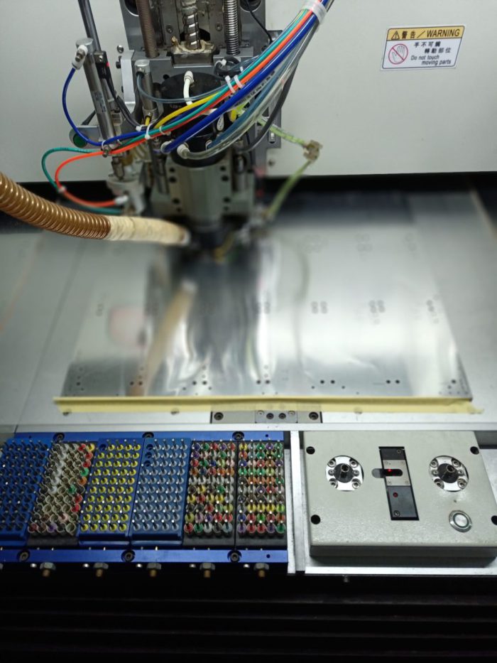
SQPCB’s Equipment and Advantages
To ensure PTH PCB reliability, SQPCB uses advanced production systems:
LDI direct imaging for circuitry and solder mask layers, automated inkjet for legends – eliminating shrinkage, misalignment, operator errors, scratches, and debris caused by outdated film methods.
In-house lamination, HASL, and ENIG plating lines – ensuring stable quality and fully controlled lead times.
This investment guarantees higher yields, superior solder mask finish, and long-term PCB reliability, even under demanding industrial or automotive conditions.
Design Considerations for PTH PCB
Hole Size & Aspect Ratio – Keep aspect ratio <10, ideally <6, to avoid uneven plating.
Hole Spacing – Maintain >0.5 mm edge-to-edge spacing to prevent electrical and mechanical risks.
Signal Integrity – Layout vias carefully to minimize loss and reflection.
Thermal Management – Distribute vias strategically to reduce board temperatures.
Common Issues and Solutions in PTH PCB
| Issue | Cause | Solution |
|---|---|---|
| Uneven Plating | Poor current control, dirty walls | Optimize plating, enhance cleaning |
| Hole Wall Cracks | Stress from drilling or weak copper | Better drilling control, thicker plating |
| Insufficient Copper Thickness | Cost-cutting practices | Ensure IPC compliance and strict QC |
| Latent Defects | Failures appear after SMT or long use | Cross-section analysis, X-Ray inspection |
Final Treatment Methods for PTH Holes
Resin Plugging – Best long-term reliability, higher cost.
Ink Plugging – Cost-effective, good for industrial PCBs.
Solder Mask Plugging – Cheaper, moderate reliability.
Via Tenting – Lowest cost, limited long-term reliability.
Choice depends on cost, reliability requirements, and operating conditions.
Conclusion
PTH PCB technology remains a cornerstone of PCB design, providing critical electrical connections, mechanical strength, and thermal stability. With the right manufacturing practices and strict compliance, PTH PCBs deliver consistent quality and long-term reliability.
SQPCB’s advanced LDI systems, in-house lamination, and ENIG plating ensure our PTH PCBs meet international IPC standards while maintaining controlled costs and delivery. With 14 years of experience, SQPCB is your trusted partner for reliable PTH PCB solutions.
FAQ
Q1: What is the standard copper thickness for PTH PCB?
A1: IPC Class 2 requires ≥18 μm; Class 3 requires ≥20 μm.
Q2: Are microvias part of PTH PCB?
A2: Yes, microvias are plated through small holes using laser drilling, widely used in HDI designs.
Q3: How can PTH quality be tested?
A3: Cross-sectioning, via resistance testing, and X-Ray inspection are common methods.
Q4: Why do some suppliers deliver poor PTH quality?
A4: Many cut costs by reducing copper plating thickness, which compromises reliability.
Q5: What advantages does SQPCB offer in PTH PCB manufacturing?
A5: SQPCB uses LDI imaging, automated inkjet, in-house lamination, and ENIG plating to deliver superior yields, high reliability, and fully controlled lead times.

- long board pcb
- Flexible PCBs
- Special PCB
- Express Printed Circuit Board
- Pcb Prototype
- LED PCB
- PCB
- Printed Circuit Board
- Pcb meaning
- Pcb manufacturer
- Rigid pcb board
- Rigid Flex PCB
 Quote
Quote
 E-mail